Display substrate and manufacturing method thereof

A production method and technology for display substrates, which are applied in nonlinear optics, instruments, optics, etc., can solve the problems of decreased display contrast, poor resolution, and affected picture quality, and achieve the effect of reducing reflections

Inactive Publication Date: 2016-04-20
BOE TECH GRP CO LTD
View PDF5 Cites 10 Cited by
  • Summary
  • Abstract
  • Description
  • Claims
  • Application Information

AI Technical Summary

Problems solved by technology

The traditional black matrix is ​​made of organic materials with poor resolution. In order to further increase the aperture ratio, metal black matrices are used in the prior art instead of organic material black matrices to reduce the width of the black matrix between two pixel units.
However, since the metal material has a certain reflectivity, the metal black matrix in the display panel will reflect light, resulting in a decrease in display contrast and affecting picture quality.

Method used


Image

  • Display substrate and manufacturing method thereof
  • Display substrate and manufacturing method thereof
  • Display substrate and manufacturing method thereof

Examples


Embodiment Construction

[0038] Specific embodiments of the present invention will be described in detail below in conjunction with the accompanying drawings. It should be understood that the specific embodiments described here are only used to illustrate and explain the present invention, and are not intended to limit the present invention.

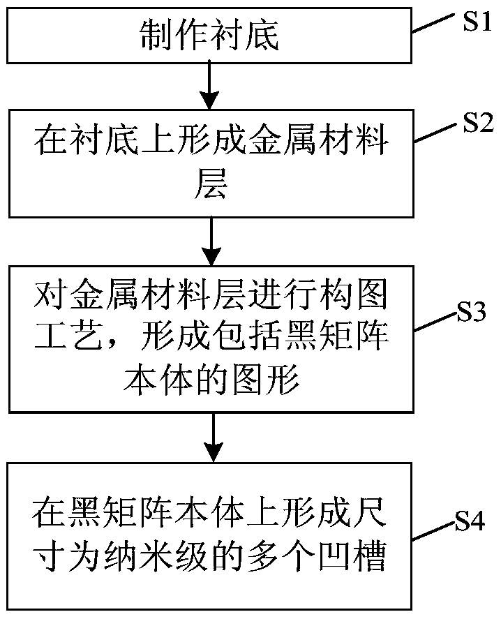
[0039] As a first aspect of the present invention, a method for manufacturing a display substrate is provided, such as figure 1 shown, including:

[0040] S1. Making a substrate.

[0041] S2, forming a metal material layer 1a on the substrate, such as Figure 4 shown.

[0042] S3, patterning the metal material layer 1a to form a pattern comprising the black matrix body 11, such as Figure 5 shown.

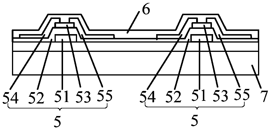
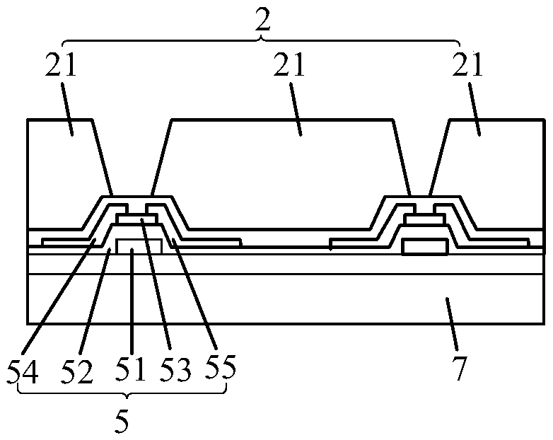
[0043] S4, forming a plurality of grooves 12 with a size of nanometer scale on the black matrix body 11 to form a pattern comprising the black matrix 1, such as Figure 6 and Figure 7 shown. Wherein, the size of the groove 12 refers to the size of the groove...


PUM

PropertyMeasurementUnit
widthaaaaaaaaaa
sizeaaaaaaaaaa
sizeaaaaaaaaaa

Abstract

The invention provides a display substrate and a manufacturing method thereof. The method includes the steps of manufacturing a substrate body, forming a metal material layer on the substrate body, and conducting the graphing process on the metal material layer to form a graph including a black matrix body, wherein a plurality of grooves with the nano-scale size are formed in the black matrix body. By means of the method, the aperture opening ratio of a display device is increased, and meanwhile the display effect of the display device can be improved.

Description

technical field [0001] The invention relates to the field of display technology, in particular to a display substrate and a manufacturing method thereof. Background technique [0002] The liquid crystal display device pastes the array substrate and the color filter substrate together through the box forming process. There will be a certain deviation between the array substrate and the color filter substrate during the box forming process. This deviation will lead to a decrease in the aperture ratio of the display device and light leakage. And other issues. In order to eliminate the deviation between the array substrate and the color filter substrate, increase the aperture ratio and reduce the cost, panel manufacturers have developed a technology in which the color filter and the black matrix are located on the array substrate, that is, COA (ColorfilmonArray) technology. The COA technology can reduce the deviation between the array substrate and the color filter substrate wh...

Claims


Application Information

Patent Timeline
Patent Type & Authority Applications(China)
IPC IPC(8): G02F1/1335
CPCG02F1/133512G02F2201/40
Inventor 何晓龙曹占锋张锋姚琪张伟孙雪菲张斌
Owner BOE TECH GRP CO LTD
Why Eureka
Try Eureka