Light emitting module of electronic equipment and manufacturing method thereof

A technology of electronic equipment and light-emitting modules, which is applied in the direction of illuminated signs, display devices, instruments, etc., and can solve problems such as unfavorable development of electronic equipment

Active Publication Date: 2018-06-01
LENOVO (BEIJING) LTD
View PDF6 Cites 0 Cited by
  • Summary
  • Abstract
  • Description
  • Claims
  • Application Information

AI Technical Summary

Problems solved by technology

This undoubtedly requires a larger system space to support, which is not conducive to the development of electronic equipment in the direction of thinning

Method used


Image

  • Light emitting module of electronic equipment and manufacturing method thereof
  • Light emitting module of electronic equipment and manufacturing method thereof

Examples


Embodiment 1

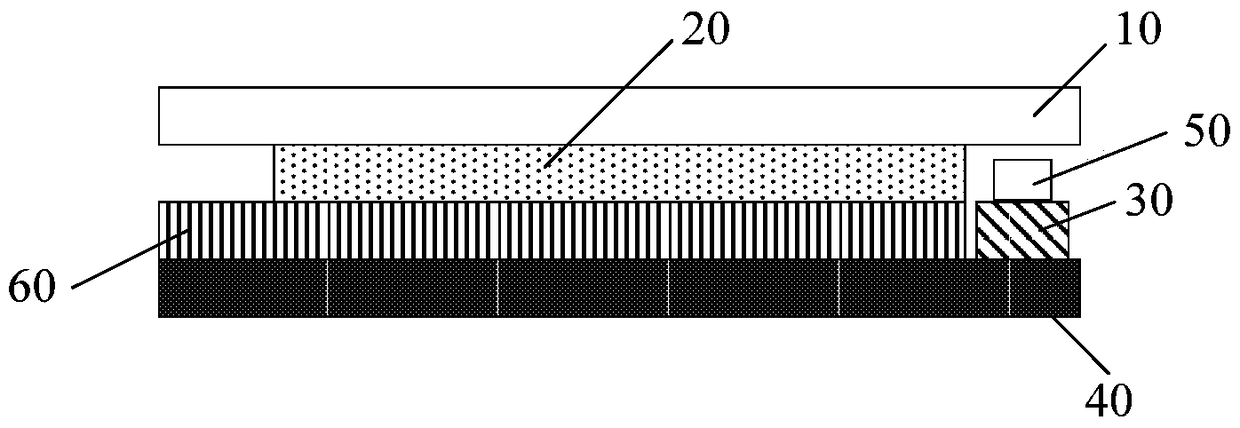
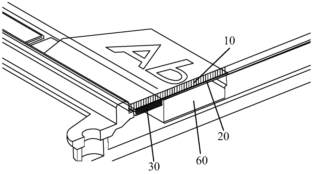
[0024] Embodiment 1 of the present invention provides a light-emitting device for electronic equipment, the light-emitting device includes a light-emitting module, such as figure 1 As shown, the light-emitting module includes: a light guide layer 20 and a PCB 30, the light guide layer 20 and the PCB 30 are arranged in a staggered position, and the PCB 30 is located in a side-by-side layer of the panel control board 60, and the guide The optical layer 20 is located above the panel control board 60 .

[0025] In order to thin the light-emitting module, the light guide layer 20 of the embodiment of the present invention can choose to use Mylar sheet, and the Mylar sheet refers to PET (polyethylene terephthalate) polyester film as the light guide layer. 20 Mylar sheet, its thickness can be 0.3mm (millimeter). Of course, the thickness of the Mylar sheet used as the light guide layer 20 is not limited to 0.3mm, and its thickness can be adjusted and selected according to actual prod...

Embodiment 2

[0033] Embodiment 2 of the present invention provides an electronic device, including the light-emitting device described in Embodiment 1 of the present invention, the light-emitting device includes a light-emitting module, the number of the light-emitting module is at least one, and the light-emitting module is set On at least one shell panel of the electronic device, or embedded in at least one shell panel of the electronic device.

Embodiment 3

[0035] Embodiment 3 of the present invention also provides a method for manufacturing a light-emitting module of an electronic device, including:

[0036] A PCB is arranged on a side-by-side layer located in the lateral direction of the panel control board, a light guide layer is arranged above the panel control board, and the light guide layer and the PCB are arranged in a dislocation manner.

[0037]Wherein, in order to thin the light-emitting module, the light guide layer of the embodiment of the present invention can choose to use Mylar sheet, and the Mylar sheet refers to PET (polyethylene terephthalate) polyester film, used as a light guide layer. The thickness of the layered Mylar sheet can be 0.3mm (millimeter). Of course, the thickness of the Mylar sheet used as the light guide layer is not limited to 0.3mm, and its thickness can be adjusted and selected according to actual product needs. For example, a Mylar sheet with a thickness of 0.3mm-0.5mm can be used as the li...


PUM


Abstract

The invention discloses a light emitting module of electronic equipment and a manufacturing method of the light emitting module. The light emitting module comprises a light conductive layer and a printed circuit board (PCB), wherein light conductive layer and the PCB are distributed in a staggered mode; the PCB is located in the traverse parallel layer of a panel control board; and the light conductive layer is located above the panel control board.

Description

technical field [0001] The invention relates to the technical field of electronic equipment, in particular to a light-emitting module of electronic equipment and a manufacturing method thereof. Background technique [0002] In the prior art, some electronic devices use a plastic / glass printing process for Logo design, which has a single display form and does not support luminous display. [0003] There are also logo designs for some electronic devices in the following way: printing a light-transmitting Logo on glass (glass), and designing transparent polycarbonate (PC, Polycarbonate) plastic parts and light-emitting diodes (LED, Light-Emitting Diode) under the glass A printed circuit board (PCB, Printed Circuit Board) is used as a light emitting module. The total thickness of the light-emitting module under this design method is usually above 2.0mm, that is, the thickness of the plastic part (at least 1.0mm) + the thickness of the LED PCB (at least 1.0mm) is usually above 2...

Claims


Application Information

Patent Timeline
Patent Type & Authority Patents(China)
IPC IPC(8): G09F13/18
CPCG09F13/18G09F2013/184
Inventor 张业欣
Owner LENOVO (BEIJING) LTD
Why Eureka
Try Eureka