Pixel arrangement structure and manufacturing method thereof and display

A pixel arrangement and manufacturing method technology, applied in the field of OLED display, can solve the problems of limiting the improvement of resolution and the ineffective use of space

Active Publication Date: 2016-05-04
KUNSHAN GO VISIONOX OPTO ELECTRONICS CO LTD
View PDF6 Cites 46 Cited by
  • Summary
  • Abstract
  • Description
  • Claims
  • Application Information

AI Technical Summary

Problems solved by technology

In this way, the space of this part of the interval cannot be effectively used, which limits the further improvement of the resolution.

Method used


Image

  • Pixel arrangement structure and manufacturing method thereof and display
  • Pixel arrangement structure and manufacturing method thereof and display
  • Pixel arrangement structure and manufacturing method thereof and display

Examples


Embodiment Construction

[0056] Further description will be given below in conjunction with the accompanying drawings and embodiments.

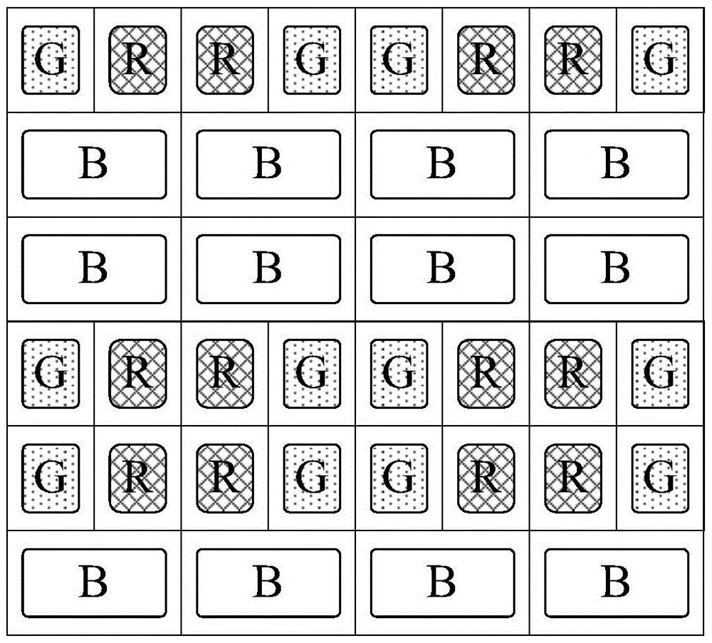
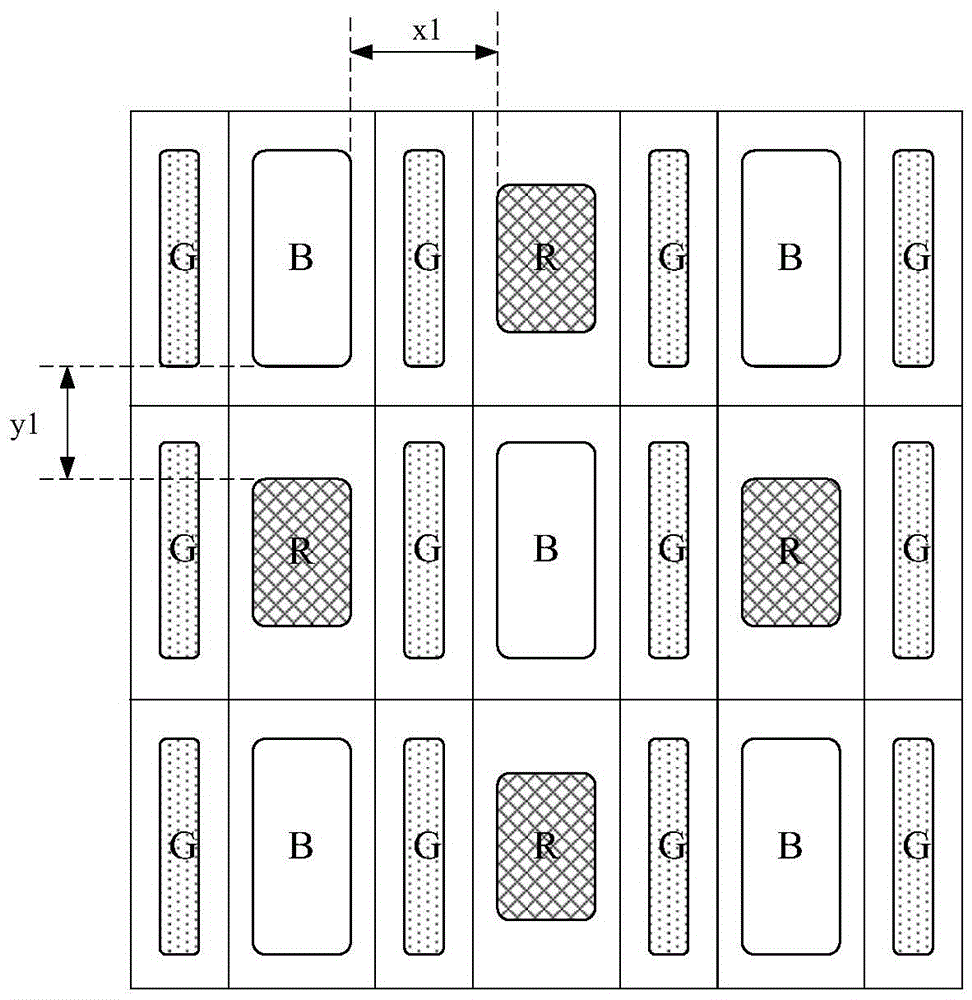
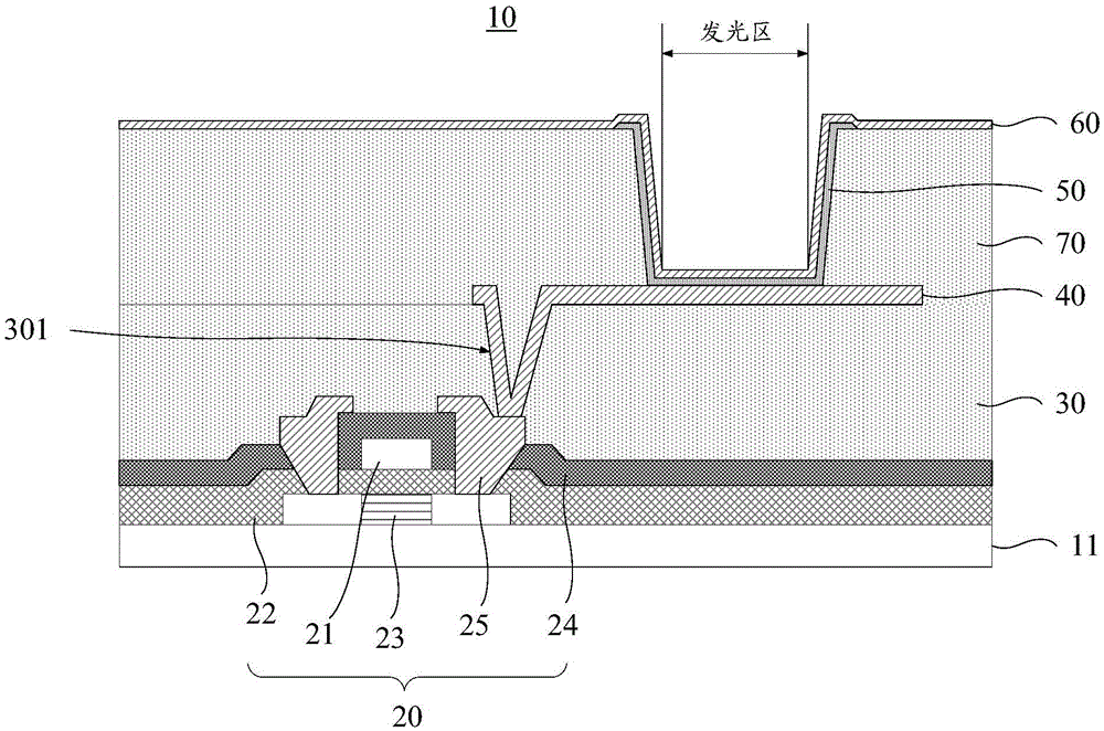
[0057] combine first Figure 3-5 Briefly explain the display principle of the self-luminous display.

[0058] image 3 A longitudinal sectional view of the organic light emitting display 10 is shown. The organic light emitting display 10 includes a substrate 11 , a driving layer 20 , a first insulating layer 30 , a first electrode 40 , a light emitting layer 50 , a second electrode 60 and a second insulating layer 70 . The driving layer 20 includes a gate electrode 21 , a gate insulating layer 22 , a semiconductor layer 23 , an interlayer insulating layer 24 and a wiring pattern 25 . The organic light emitting display 10 is a top emission display device, that is, light is emitted from the second electrode 60 . The first electrode 40 is electrically connected to the lead pattern 25 through a through hole provided on the first insulating layer 30 . An opening is f...


PUM


Abstract

The invention relates to a pixel arrangement structure, which comprises a plurality of first repeating unit and second repeating units, wherein the first repeating units and the second repeating units alternately repeat in a row direction and a column direction in sequence to form a matrix arrangement; each first repeating unit comprises two green sub-pixels and a blue sub-pixel; each second repeating unit comprises two green sub-pixels and a red sub-pixel; and each red sub-pixel and each blue sub-pixel are shared by four green sub-pixels to form four pixel units. The invention further relates to a display employing the pixel arrangement structure and a manufacturing method of the pixel arrangement structure. The pixel arrangement structure and the display can provide relatively high display resolution.

Description

technical field [0001] The invention relates to OLED display technology, in particular to a pixel arrangement structure, a manufacturing method thereof and a display. Background technique [0002] Since high resolution can display finer colors and more image details, which can bring better visual experience to users, display devices with high resolution are increasingly favored by users. [0003] The current display technology adopts the same basic principles, that is, a pixel is composed of red, green, and blue sub-pixels, and the color of each pixel can be adjusted from red, green, and blue according to different brightness levels. Come out, the displayed image is actually a collection of display states of pixels. When there are more pixels per unit area, more image details can be represented. [0004] Unlike display devices that use backlights that rely on filters to obtain sub-pixels of different colors, self-illuminating display devices, each sub-pixel relies on the e...

Claims


Application Information

Patent Timeline
Patent Type & Authority Applications(China)
IPC IPC(8): H01L27/32H01L51/56
CPCH10K59/353H10K71/00
Inventor 刘将魏朝刚
Owner KUNSHAN GO VISIONOX OPTO ELECTRONICS CO LTD
Why Eureka
Try Eureka