Method for punching dovetail groove in front surface of lead frame of semiconductor

A technology of lead frame and dovetail groove, which is applied in the direction of semiconductor devices, semiconductor/solid-state device manufacturing, semiconductor/solid-state device components, etc., can solve the problems such as poor surface flatness of products, achieve improved reliability, good dovetail structural strength, Effect of reducing material stress variation

Active Publication Date: 2016-05-11
SICHUAN JINWAN ELECTRONICS
View PDF4 Cites 2 Cited by
  • Summary
  • Abstract
  • Description
  • Claims
  • Application Information

AI Technical Summary

Problems solved by technology

[0004] In view of this, the object of the present invention is to provide a semiconductor lead frame front dovetail punching method to solve the problem of poor surface flatness of the product after the dovetail groove is formed

Method used


Image

  • Method for punching dovetail groove in front surface of lead frame of semiconductor
  • Method for punching dovetail groove in front surface of lead frame of semiconductor
  • Method for punching dovetail groove in front surface of lead frame of semiconductor

Examples


Embodiment Construction

[0021] The present invention will be described in further detail below through specific embodiments and in conjunction with the accompanying drawings.

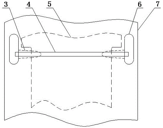
[0022] A stamping method for dovetail slots on the front of a semiconductor lead frame, including the following:

[0023] A. Process the lead frame blank, pre-cut both sides of the lead frame blank at one time, and punch a strip hole on both sides of the lead frame blank;

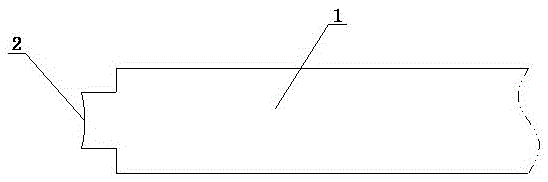
[0024] B. Press the rectangular groove: press the material through the mold, use the punch I with a rectangular cross-section to vertically extrude the lead frame blank, and obtain a rectangular groove with a rectangular cross-section;

[0025] C. Pressing the dovetail groove: use the convex die II with a concave arc at the top of the section to vertically extrude the center of the rectangular groove formed in the previous step to form the dovetail groove;

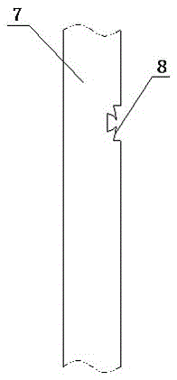
[0026] D. Pre-cut dovetail groove: cut off the excess material on both sides of the dovetail gr...


PUM


Abstract

The invention discloses a method for punching a dovetail groove in the front surface of a lead frame of a semiconductor, and relates to the technical field of manufacturing of electronic components of the semiconductor. The method comprises the following contents: (A) processing and fabricating a lead frame blank, precutting two sides of the lead frame blank once and punching a strip-shaped hole in each of two sides of the lead frame blank; (B) pressing a rectangular groove, namely pressing materials through a mold and vertically extruding the lead frame blank with a convex mold I with a rectangular section to obtain a rectangular groove with the rectangular section; (C) punching the dovetail groove, namely vertically extruding the central position of the rectangular groove molded in the previous step with a convex mold II with a concave arc top part in the section and molding the dovetail groove; (D) precutting the dovetail groove, namely cutting off excessive materials at two sides of the dovetail groove; and (E) accurately cutting the dovetail groove, namely accurately cutting two ends of the dovetail groove. Through the steps, the dovetail groove with good strength and an optimal structure is obtained; and meanwhile, the problem of poor flatness of the surface after the dovetail groove is formed in the lead frame of the semiconductor is solved.

Description

technical field [0001] The invention relates to the technical field of manufacturing semiconductor electronic components, in particular to a stamping method for a front dovetail groove of a semiconductor lead frame. Background technique [0002] As the chip carrier of integrated circuits, the lead frame is a key structural part that realizes the electrical connection between the lead-out end of the chip's internal circuit and the outer lead by means of bonding materials (gold wire, aluminum wire, copper wire) to form an electrical circuit. When it comes to the bridge function of connecting with external wires, most semiconductor integrated blocks need to use lead frames, which are important basic materials in the electronic information industry. At present, semiconductor electronic components are usually assembled from chips, plastic packaged parts, gold wires or aluminum wires, and lead frames. In order to improve the efficiency of automated production, lead frames are gene...

Claims


Application Information

Patent Timeline
Patent Type & Authority Applications(China)
IPC IPC(8): H01L21/48H01L23/495
CPCH01L21/4842H01L23/49548
Inventor 黄斌任俊
Owner SICHUAN JINWAN ELECTRONICS
Why Eureka
Try Eureka