Array substrate, manufacturing method thereof, and display device

A technology for array substrates and manufacturing methods, which is applied in the display field, can solve problems such as poor contact, the size of via holes cannot be too small, and the production yield of array substrates is reduced, so as to achieve the effects of improving production yield and opening ratio

Active Publication Date: 2018-11-02
CHONGQING BOE OPTOELECTRONICS +1
View PDF3 Cites 0 Cited by
  • Summary
  • Abstract
  • Description
  • Claims
  • Application Information

AI Technical Summary

Problems solved by technology

[0003] In the manufacturing process of the existing array substrate, PVD (Physical Vapor Deposition, Physical Vapor Deposition) method is usually used to deposit a conductive layer at the via hole of the insulating layer, so as to realize the connection between the conductive layer and the conductive pattern under the insulating layer. This method requires that the size of the via hole should not be too small. If the size of the via hole is too small, poor contact will easily occur between the conductive layer and the conductive pattern formed at the via hole, resulting in a decrease in the production yield of the array substrate.

Method used


Image

  • Array substrate, manufacturing method thereof, and display device
  • Array substrate, manufacturing method thereof, and display device
  • Array substrate, manufacturing method thereof, and display device

Examples


Embodiment 1

[0039] This embodiment provides a method for manufacturing an array substrate, including:

[0040] forming a first conductive pattern on the substrate;

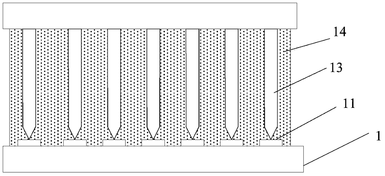
[0041] forming an insulating layer including a via hole on the substrate formed with the first conductive pattern, and at least part of the first conductive pattern is exposed at the via hole;

[0042] immersing the substrate formed with the insulating layer in a metal salt solution;

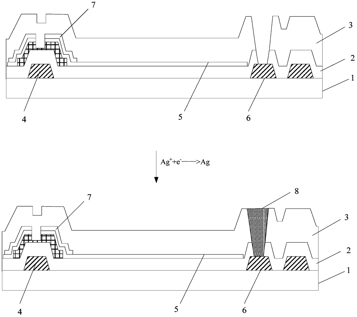
[0043] Input an electrical signal to the first conductive pattern, so that after the metal salt solution at the via hole contacts the first conductive pattern, the metal ions in the metal salt solution are reduced and deposited at the via hole to form a conductive connection department.

[0044] In this embodiment, the array substrate formed with the insulating layer is immersed in the metal salt solution, and an electric signal is input to the first conductive pattern exposed at the via hole of the insulating layer, and the metal salt soluti...

Embodiment 2

[0060] This embodiment provides an array substrate, which is manufactured by using the above manufacturing method, an insulating layer including a via hole is formed on the array substrate, and a conductive connection to the first conductive pattern is formed at the via hole department.

[0061]The technical solution of this embodiment does not have the problem of poor contact between the first conductive pattern and the conductive connection part, and can improve the production yield of the array substrate; and the technical solution of this embodiment does not require the size of the via hole, and can The conductive connection part is formed at the via hole, and the size of the via hole can be set relatively small, thereby increasing the aperture ratio of the array substrate.

Embodiment 3

[0063] This embodiment provides a display device, including the above-mentioned array substrate. The display device can be any product or component with display function such as LCD TV, liquid crystal display, digital photo frame, mobile phone, tablet computer, etc., wherein the display device also includes a flexible circuit board, a printed circuit board and a backplane.


PUM


Abstract

The invention provides an array substrate, a fabrication method thereof and a display device, belonging to the technical field of display. The fabrication method of the array substrate comprises the following steps of forming a first conductive pattern on the substrate; forming an insulation layer comprising via holes on the substrate provided with the first conductive pattern, wherein at least one part of the first conductive pattern is exposed out of the via holes; immersing the substrate provided with the insulation layer in a metal salt solution; and inputting an electric signal to the first conductive pattern so as to make metal ions in the metal salt solution reduced and deposited in the via holes to form a conductive connection part after the metal salt solution in the via holes is in contact with the first conductive pattern. With the technical scheme provided by the invention, the electrical connection status of the array substrate in the via holes can be optimized, and the production yield of the array substrate is improved.

Description

technical field [0001] The present invention relates to the field of display technology, in particular to an array substrate, a manufacturing method thereof, and a display device. Background technique [0002] With the development of display technology, the PPI (pixel density) of the display panel is gradually increasing, the size of TFT (thin film transistor) is getting smaller and smaller, and the corresponding Via hole (via hole) size is also getting smaller. [0003] In the manufacturing process of the existing array substrate, PVD (Physical Vapor Deposition, Physical Vapor Deposition) method is usually used to deposit a conductive layer at the via hole of the insulating layer, so as to realize the connection between the conductive layer and the conductive pattern under the insulating layer. This method requires that the size of the via hole should not be too small. If the size of the via hole is too small, poor contact will easily occur between the conductive layer and ...

Claims


Application Information

Patent Timeline
Patent Type & Authority Patents(China)
IPC IPC(8): H01L21/84H01L27/12H01L21/77
CPCH01L27/1244H01L27/1259
Inventor 文江鸿齐智坚张智唐滔良陈帅王志会钱谦唐秀珠苟中平陈刚
Owner CHONGQING BOE OPTOELECTRONICS
Why Eureka
Try Eureka