Film transistor, array substrate and liquid crystal panel

A thin-film transistor and thin-film technology, applied in the field of liquid crystal display, can solve problems affecting the display quality of liquid crystal panels, achieve the effects of reducing light leakage current, reducing dark state leakage current, and improving display quality

Inactive Publication Date: 2016-05-11
TCL CHINA STAR OPTOELECTRONICS TECH CO LTD
View PDF3 Cites 1 Cited by
  • Summary
  • Abstract
  • Description
  • Claims
  • Application Information

AI Technical Summary

Problems solved by technology

[0003] In order to make the TFT have a smaller dark-state leakage current, a method in the prior art is: an amorphous phase ohmic contact layer is introduced between the source and drain electrodes and the semiconductor layer, the amorphous phase ohmic contact layer includes an amorphous phase film, The amorphous phase film is formed by doping the semiconductor layer with a high concentration of P element. Although the amorphous phase ohmic contact layer can effectively reduce the dark state leakage current of the TFT, it is very easy to cause the TFT to appear as figure 1 The higher photoleakage current shown, which in turn affects the display quality of the LCD panel

Method used


Image

  • Film transistor, array substrate and liquid crystal panel
  • Film transistor, array substrate and liquid crystal panel
  • Film transistor, array substrate and liquid crystal panel

Examples


Embodiment Construction

[0022] Certain words are used to refer to specific components in the description and claims, and those skilled in the art should understand that manufacturers may use different terms to refer to the same component. The specification and claims do not use the difference in name as a way to distinguish components, but use the difference in function of components as a basis for distinction. The present invention will be described in detail below in conjunction with the accompanying drawings and embodiments.

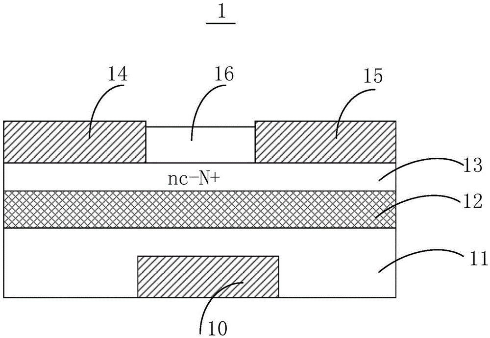
[0023] figure 2 is a schematic structural diagram of a thin film transistor according to the first embodiment of the present invention. like figure 2 As shown, the thin film transistor 1 includes: a gate 10, a gate insulating layer 11 covering the gate 10, a semiconductor layer 12 and an ohmic contact layer 13 in sequence, a source 14 and a drain formed on the ohmic contact layer 13 and arranged at intervals 15.

[0024] Specifically, the gate insulating layer 11 is di...


PUM


Abstract

The invention discloses a film transistor, an array substrate and a liquid crystal panel. The film transistor comprises a grid, an insulating layer, a semiconductor layer and an ohmic contact layer, a source electrode, and a leakage electrode, wherein the insulating layer, the semiconductor layer and the ohmic contact layer successively cover the grid, and the source electrode and the leakage electrode are formed on the ohmic contact layer and arranged at intervals, and the ohmic contact layer is a nanocrystalline phase ohmic contact layer. Through above arrangment, the invention can reduces the light leakage current of the film transistor while reducing the dark state leakage current and reduces the light lekage current of the film transistor so as to improve the display quality of the display panel.

Description

technical field [0001] The invention relates to the field of liquid crystal display, in particular to a thin film transistor, an array substrate and a liquid crystal panel. Background technique [0002] With the development of science and technology, liquid crystal display technology has been developed rapidly. As an important part of liquid crystal display technology, thin film transistors (TFTs) need to have more and more excellent performances. [0003] In order to make the TFT have a smaller dark-state leakage current, a method in the prior art is: an amorphous phase ohmic contact layer is introduced between the source and drain electrodes and the semiconductor layer, the amorphous phase ohmic contact layer includes an amorphous phase film, The amorphous phase film is formed by doping the semiconductor layer with a high concentration of P element. Although the amorphous phase ohmic contact layer can effectively reduce the dark state leakage current of the TFT, it is ver...

Claims


Application Information

Patent Timeline
IPC IPC(8): H01L29/786H01L27/12
CPCH01L29/78609H01L27/1229
Inventor 蒙艳红吕晓文李文辉张合静石龙强李珊
Owner TCL CHINA STAR OPTOELECTRONICS TECH CO LTD
Why Eureka
Try Eureka