
Active switch, manufacture method thereof, and display device

A manufacturing method and switching technology, applied in semiconductor/solid-state device manufacturing, electrical components, transistors, etc., can solve problems such as increased light leakage current

Inactive Publication Date: 2019-04-12
HKC CORP LTD
View PDF12 Cites 0 Cited by
  • Summary
  • Abstract
  • Description
  • Claims
  • Application Information

AI Technical Summary

Problems solved by technology

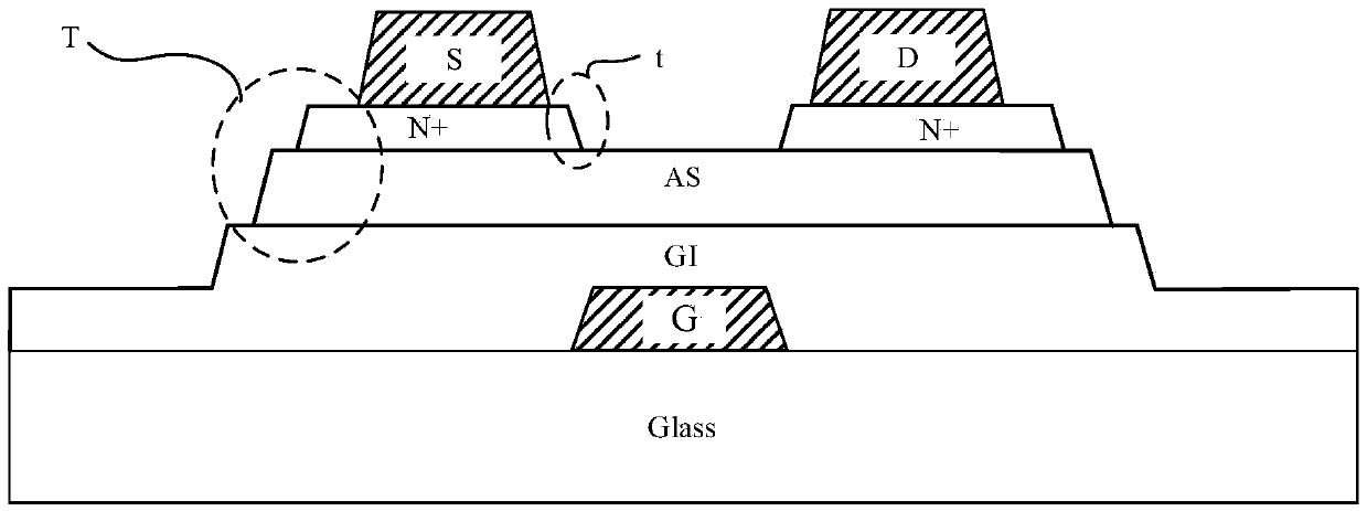
[0004] Based on this, it is necessary to provide an active switch, a manufacturing method thereof, and a display device for the problem that a switching device made by using a 4-mask process has a large Tail (tail), which leads to an increase in light leakage current.

Method used


Image

  • Active switch, manufacture method thereof, and display device
  • Active switch, manufacture method thereof, and display device
  • Active switch, manufacture method thereof, and display device

Examples


Embodiment Construction

[0041] In order to facilitate the understanding of the present application, the present application will be described more fully below with reference to the relevant drawings. Alternative embodiments of the application are presented in the drawings. However, the present application can be embodied in many different forms and is not limited to the embodiments described herein. On the contrary, the purpose of providing these embodiments is to make the disclosure of the application more thorough and comprehensive.

[0042] It should be noted that when an element is referred to as being “fixed” to another element, it can be directly on the other element or there can also be an intervening element. When an element is referred to as being "connected to" another element, it can be directly connected to the other element or intervening elements may also be present. The terms "vertical," "horizontal," "left," "right," and similar expressions are used herein for purposes of illustrati...


PUM

PropertyMeasurementUnit
thicknessaaaaaaaaaa
thicknessaaaaaaaaaa

Abstract

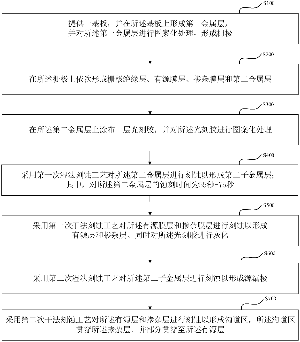
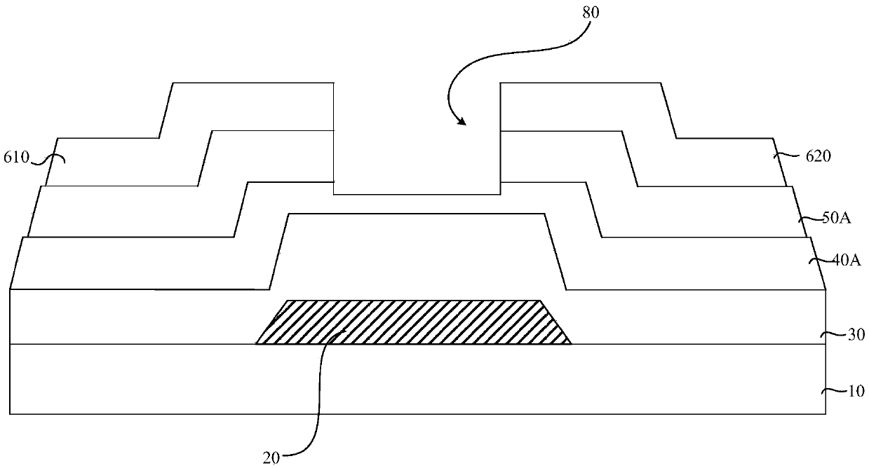
The invention relates to an active switch, a manufacture method thereof, and a display device. The manufacture method for the active switch comprises the following steps that: providing a substrate, and forming a grid electrode on the substrate; forming a grid electrode insulation layer, an active membrane layer, a doped membrane layer and a second metal layer on the grid electrode in sequence; adopting a first-time wet method etching technology to etch the second metal layer to form a second sub-metal layer, wherein the etching time of the second metal layer is 55-75 seconds; adopting a first-time dry method etching technology to etch the active membrane layer and the doped membrane layer to form an active layer and a doping layer, and meanwhile, carrying out ashing on photoresist; adopting a second wet method etching technology to etch the second sub-metal layer to form a source and drain electrode; and adopting a second dry method etching technology to etch the active layer and thedoped layer to form a channel region. By use of the manufacture method, the light leakage current of an active switch device can be effectively lowered, and a ghost phenomenon is eliminated.

Description

technical field [0001] The present application relates to the field of display technology, in particular to an active switch, a manufacturing method thereof, and a display device. Background technique [0002] As a switching device that plays a very important role in the working performance of the display panel, it is a very important key device in the display technology. With the iterative development of display technology, display devices with higher performance, high image quality and large size have become a development trend, and are also factors that directly affect user viewing experience and shopping experience. In terms of high performance, if a display device is to have higher performance, one aspect requires high-performance switching devices in the display device. [0003] In the general switching device manufacturing process, it can be divided into 5-mask process and 4-mask process. Compared with the 5-mask process, the 4-mask process reduces the photolithograp...

Claims


Application Information

Patent Timeline
Patent Type & Authority Applications(China)
IPC IPC(8): H01L21/336H01L29/786H01L29/423H01L21/28
CPCH01L29/401H01L29/42384H01L29/66765H01L29/66772H01L29/78603H01L29/78669
Inventor 莫琼花
Owner HKC CORP LTD
Learn More