Pixel structure of in-plane switching LCD panel and manufacturing method thereof

A liquid crystal display panel and pixel structure technology, applied in semiconductor/solid-state device manufacturing, transistors, static indicators, etc., can solve problems such as long manufacturing process time, poor liquid crystal alignment, and liquid crystal molecules cannot rotate normally, so as to reduce poor alignment , reduce manufacturing costs, and reduce the effect of height gap

Inactive Publication Date: 2006-07-12
CHUNGHWA PICTURE TUBES LTD
View PDF0 Cites 0 Cited by
  • Summary
  • Abstract
  • Description
  • Claims
  • Application Information

AI Technical Summary

Problems solved by technology

In this way, during the alignment process, due to the included angle θ between the alignment direction D of the alignment film 150 and the extension direction of the electrodes 130 and 140, poor liquid crystal alignment may occur in the regions 144 on both sides of the electrodes, resulting in liquid crystal molecules Can't rotate properly, thus reducing the display quality of the LCD monitor
In addition, the known manufacturing process of the pixel structure of the plane orientation switching liquid crystal display panel usually requires five photomask manufacturing processes, and when defining the source / drain, part of the channel layer may also be etched, so not only the manufacturing process time Longer, and the pass rate of its manufacturing process can not be effectively improved

Method used


Image

  • Pixel structure of in-plane switching LCD panel and manufacturing method thereof
  • Pixel structure of in-plane switching LCD panel and manufacturing method thereof
  • Pixel structure of in-plane switching LCD panel and manufacturing method thereof

Examples


Embodiment Construction

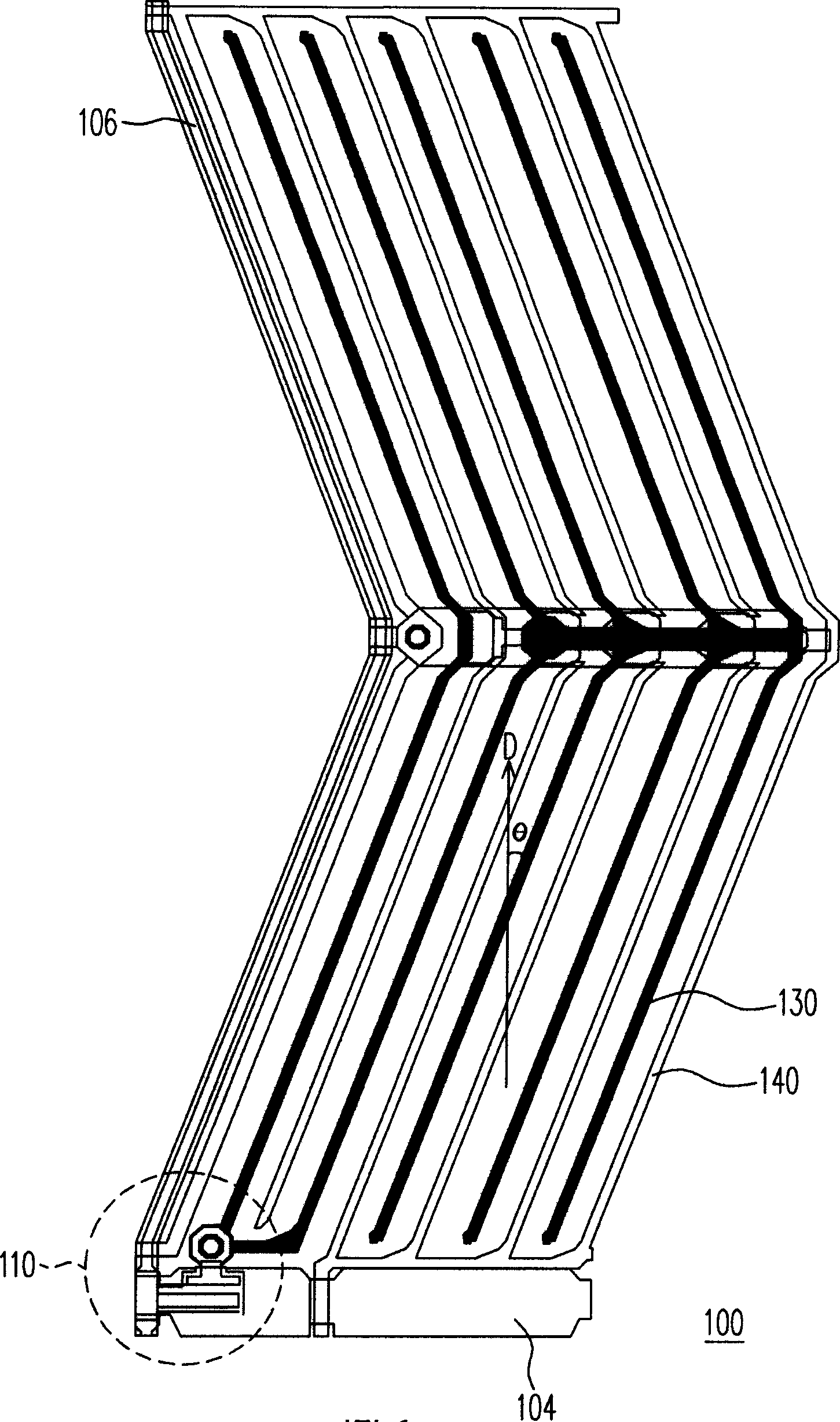
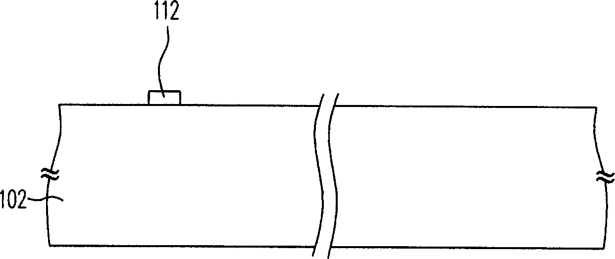
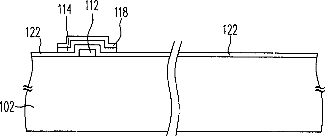
[0013] image 3 It is a schematic cross-sectional view of a pixel structure of a plane orientation switching liquid crystal display of the present invention. Please refer to image 3 The pixel structure 300 is constructed on a substrate 302, such as a glass substrate, and the pixel structure 300 is driven by, for example, scanning lines and data lines (not shown in the figure). The pixel structure 300 includes a thin film transistor 310, a dielectric layer 320, a plurality of driving electrodes 330 and a plurality of shared electrodes 340, wherein the thin film transistor 310 is disposed on a substrate 302 and connected to a scan line and a data line (not shown in the figure) . In addition, the dielectric layer 320 is, for example, formed by extending the gate insulating layer 322 and the protective layer 324 inside the thin film transistor 310, wherein the dielectric layer 320 has a plurality of strip openings 324b, and the driving electrode 330 and the common electrode 340...


PUM


Abstract

The invention discloses a pixel structure of plane direction conversion liquid crystal panel, which comprises the following parts: film transistor, dielectric layer, multiple driving electrodes and multiple sharing electrodes, wherein the film transistor is set on the base plate, which is connected to the scanning line and data line; the driving electrode and sharing electrode are inserted in the dielectric layer with mutual interpenetration allocation; the driving electrode connects the film transistor; the pixel structure can improve the imperfect direction-mating condition of two electrode sides, which reduces the needed photomask quantity in the manufacturing craft.

Description

technical field [0001] The present invention relates to a pixel structure and a manufacturing method thereof, and in particular to a pixel structure of a plane direction switching liquid crystal display panel and a manufacturing method thereof. Background technique [0002] With the high development of multimedia technology, most of the transmission of image information has now been converted from analog to digital transmission, and in order to match the modern life style, the volume of video or image devices is also becoming thinner and thinner. Although the traditional cathode ray tube (Cathode Ray Tube, CRT) display has the advantages of excellent display quality and low cost, due to the structure of its internal electron gun, the display cannot meet the requirements of thinning, light weight and low power consumption, and There are also problems such as radiation damage to the eyes when the user watches. Therefore, with the maturity of optoelectronic technology and semi...

Claims


Application Information

Patent Timeline
Patent Type & Authority Applications(China)
IPC IPC(8): G02F1/136G02F1/133H01L29/786H01L21/00
Inventor 周瑞渊王明宗邱献清
Owner CHUNGHWA PICTURE TUBES LTD
Why Eureka
Try Eureka