A kind of manufacturing method of gold finger card board

A manufacturing method and technology for gold fingers, which are applied in the direction of electrical connection of printed components, printed circuit components, and the formation of electrical connection of printed components, can solve the problems of increasing resource consumption and production costs, increasing the thickness of gold fingers, and disadvantageous gold finger insertion. The card board structure and other issues can increase energy consumption and production costs, change processes and processes, and ensure universality.

Active Publication Date: 2018-09-04
NEW FOUNDER HLDG DEV LLC +1
View PDF3 Cites 0 Cited by
  • Summary
  • Abstract
  • Description
  • Claims
  • Application Information

AI Technical Summary

Problems solved by technology

Obviously, methods 1 and 2 will greatly increase resource consumption and increase production costs, and are not conducive to the compact structure of the gold finger card board; method 3 will increase the thickness of the board. According to the design of the conventional gold finger card board, the board thickness The thickness of the gold fingers will also increase for the added card boards, resulting in poor versatility of the gold finger boards

Method used


Image

  • A kind of manufacturing method of gold finger card board
  • A kind of manufacturing method of gold finger card board
  • A kind of manufacturing method of gold finger card board

Examples


Embodiment 1

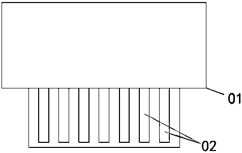
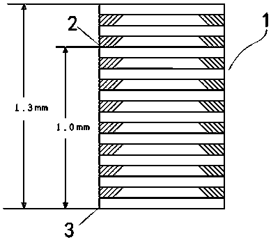
[0045] This embodiment provides a gold finger plug-in card board, which includes a 10-layer circuit board as an example, including a card board body 1 with 10 layers of circuit board layers and a gold finger 4 arranged on one side of the card body 1 , the golden fingers 4 are respectively electrically connected to the circuit board layer through the top finger wiring layer 2 and the bottom finger wiring layer 3 opposite to the top finger wiring layer 2, specifically as image 3 As shown, the top finger wiring layer 2 and the bottom finger wiring layer 3 of the gold finger 4 are respectively laid on the third circuit board of the circuit board layer (such as Figure 7 shown in the area of ​​C) and the bottom circuit board (such as Figure 9 (shown in the area of ​​part E in the middle); along the layer stacking direction of the card board main body 1, the thickness between the top of the top finger wiring layer 2 and the bottom of the bottom finger wiring layer 3 is less than t...

Embodiment 2

[0056] This embodiment provides a gold finger card board, which is a modification on the basis of Embodiment 1, the difference is that: Figure 10 As shown, the top finger wiring layer 2 and the bottom finger wiring layer 3 of the golden finger 4 are respectively laid on the top circuit board and the eighth circuit board of the circuit board layer.

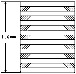
[0057] In this embodiment, the thickness between the top of the top finger wiring layer 2 and the bottom of the bottom finger wiring layer 3 is 1.0 mm, and the thickness of the cardboard main body 1 is 1.3 mm. Similarly, the above-mentioned thicknesses of 1.0 mm and 1.3 mm are only an example of this embodiment, and should not be understood as a limitation of this embodiment. If necessary, the top finger wiring layer 2 and the bottom finger wiring layer 3 The thickness between the bottoms can be other thicknesses, and the thickness of the card board main body 1 can also be set to an appropriate thickness according to needs. In ad...

Embodiment 3

[0066] This embodiment provides a gold finger card board, which is a modification on the basis of Embodiment 1, the difference is that: Figure 11 As shown, the top finger wiring layer 2 and the bottom finger wiring layer 3 of the golden finger 4 are respectively laid on the second-layer circuit board and the ninth-layer circuit board of the circuit board layer.

[0067] In this embodiment, the thickness between the top of the top finger wiring layer 2 and the bottom of the bottom finger wiring layer 3 is 1.0 mm, and the thickness of the cardboard main body 1 is 1.3 mm. Similarly, the above-mentioned thicknesses of 1.0 mm and 1.3 mm are only an example of this embodiment, and should not be understood as a limitation of this embodiment. If necessary, the top finger wiring layer 2 and the bottom finger wiring layer 3 The thickness between the bottoms can be other thicknesses, and the thickness of the card board main body 1 can also be set to an appropriate thickness according to...


PUM


Abstract

The invention provides a metal-finger plugging board and a manufacturing method thereof. The metal-finger plugging board comprises a main board body having a circuit board layer and a metal finger arranged at one side of the main board body. The metal finger is connected with the circuit board layer electrically by a top finger wiring layer and a bottom finger wiring layer opposite to the top finger wiring layer. The thickness between the top of the top finger wiring layer and the bottom of the bottom finger wiring layer is less than the thickness of the main board body along the lamination direction of the circuit board layer of the main board body. According to the invention, the design concept of the metal-finger plugging board enables the limitation of the conventional way to be broken through; and the traditional way of arranging the top finger wiring layer and the bottom finger wiring layer of the plugging head of the metal finger at positions, approaching the board edges, of the top surface and the bottom surface of the circuit board layer is changed. Therefore, the structure of the metal-finger plugging board is changed and the process for producing the metal-finger plugging board is changed. With the metal-finger plugging board, the function extending demand can be satisfied; the universality is high; and the production cost is not increased substantially.

Description

technical field [0001] The invention relates to a golden finger card board and a manufacturing method thereof, and belongs to the technical field of design and production of gold finger card boards. Background technique [0002] With the rapid development of electronic technology, the trend of small, multi-functional, portable and easy-to-carry electronic products has become a trend, and most PCB boards are developing in the direction of high-layer and high-density multilayer circuit board design. In the optical fiber communication of electronic products, there is an upgradeable signal processing device, which is used for temporary data storage, data exchange and data calculation during the process of converting optical signals into electrical signals. Since this device needs to be upgraded frequently, it is generally designed A gold finger card board with a thickness of 1.0mm is formed. [0003] The role of the gold finger is to realize the connection of circuits and trans...

Claims


Application Information

Patent Timeline
Patent Type & Authority Patents(China)
IPC IPC(8): H05K1/11H05K3/40
Inventor 葛春朱兴华任军成
Owner NEW FOUNDER HLDG DEV LLC
Why Eureka
Try Eureka