Planar waveguide imaging device and method

A planar waveguide and imaging device technology, applied in the field of planar waveguide imaging devices, can solve the problem of uniform brightness of planar waveguide imaging, and achieve the effects of improving human eye comfort, avoiding unclear images, and expanding the field of view.

Active Publication Date: 2016-06-08
SHANGHAI RAYPAI PHOTONIC CRYSTAL LTD
View PDF6 Cites 5 Cited by
  • Summary
  • Abstract
  • Description
  • Claims
  • Application Information

AI Technical Summary

Problems solved by technology

[0003] In order to solve the technical problem of uniformity of brightness in planar waveguide imaging, the present invention provides a planar waveguide imaging device and method

Method used


Image

  • Planar waveguide imaging device and method
  • Planar waveguide imaging device and method
  • Planar waveguide imaging device and method

Examples


Embodiment Construction

[0036] The present invention will be further explained below in conjunction with the accompanying drawings and specific embodiments.

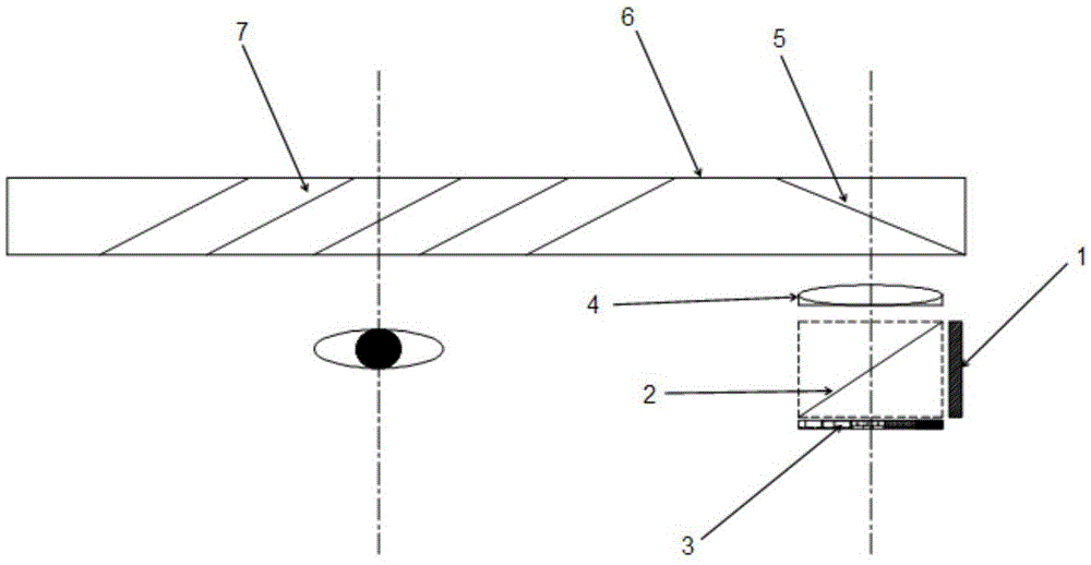
[0037] Planar waveguide imaging setup, including:

[0038] An illuminating light source 1, which emits exponentially distributed S light;

[0039] A grating film 2, the grating film 2 reflects S light;

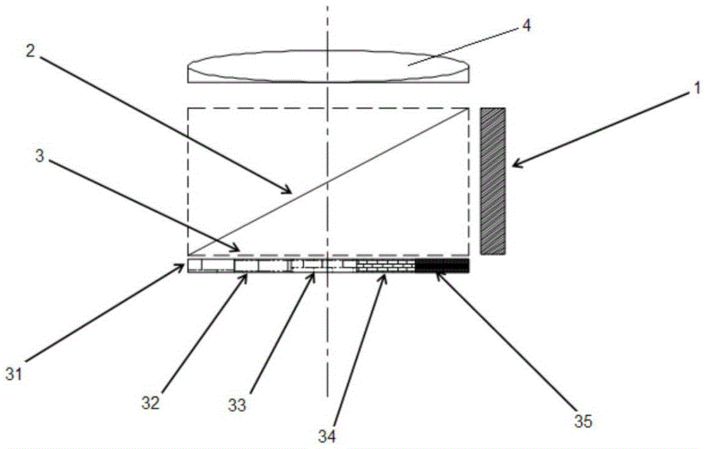
[0040] The image source 3, the S light reflected by the grating film 2 is received by the image source 3, the S light is modulated by the image source 3 into P light, and the P light is transmitted by the grating film 2;

[0041] An optical collimation system 4, the optical collimation system 4 is used to collimate the P light emitted from each point of the image source 3;

[0042] a light wave coupling input surface 5, the light wave coupling input surface 5 is used to reflect the P light entering the planar waveguide; and

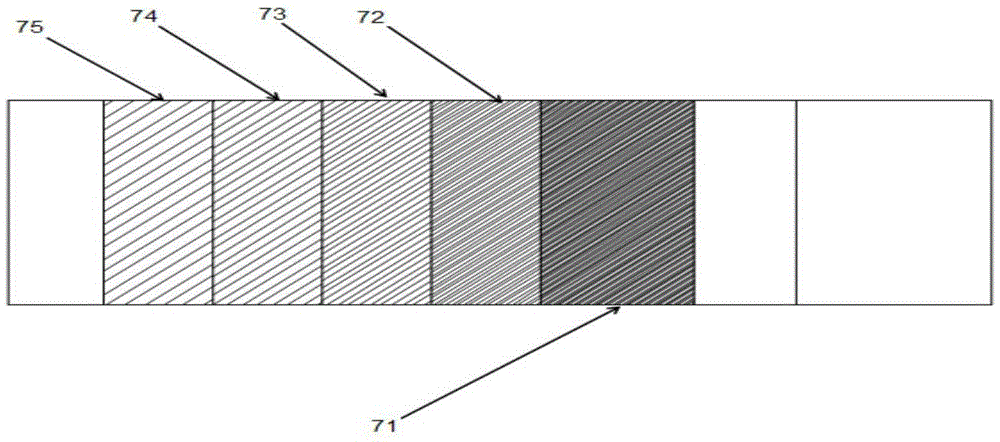
[0043] The light wave coupling output surface 7, a plurality of light wave coupling output surfaces 7 are placed in p...


PUM


Abstract

The invention discloses a planar waveguide imaging device and method. The device comprises a lighting source, an optical grating film, an image source, an optical alignment system, an optical wave coupling input surface, a planar waveguide substrate and optical wave coupling output surfaces, wherein the lighting source is used for emitting optical waves distributed in the exponential order, the optical grating film is used for reflecting the optical waves emitted by the lighting source, the image source is used for modulating the optical waves reflected by the optical grating film, the modulated optical waves can be transmitted through the optical grating film, the optical alignment system is used for alignment of the optical waves transmitted by the optical grating film, the optical wave coupling input surface is used for coupling the aligned optical waves into a planar waveguide, the planar waveguide substrate is used for conducting reflection propagation on the input coupled optical waves to form total reflection optical waves, and the optical wave coupling output surfaces are used for expanding the view field and outputting the coupled optical waves out of the planar waveguide substrate. The device and method can improve the luminance uniformity of output images of a wearable waveguide, and designing and machining difficulty is reduced.

Description

technical field [0001] The present invention relates to an imaging device and method, in particular to a planar waveguide imaging device and method. Background technique [0002] At present, in the field of planar waveguide imaging, multiple parallel reflective surfaces are used to reflect and output a large field of view image from bright to dark, and the brightness of the image is uneven, which makes the human eye uncomfortable. Patent No. US7576916B2 describes the use of multiple reflective surfaces with different reflectivity at different incident angles to solve the problem of image inhomogeneity. A lot of money invested. Contents of the invention [0003] In order to solve the technical problem of flat waveguide imaging brightness uniformity, the present invention provides a planar waveguide imaging device and method. [0004] In order to achieve the above object, the first aspect of the present invention provides a planar waveguide imaging device, including: ...

Claims


Application Information

Patent Timeline
Patent Type & Authority Applications(China)
IPC IPC(8): G02B27/01G02B27/00
CPCG02B27/0081G02B27/0101
Inventor 张圣军张庆
Owner SHANGHAI RAYPAI PHOTONIC CRYSTAL LTD
Why Eureka
Try Eureka