Display device and chip binding method thereof

A technology for display devices and chips, which is applied to identification devices, static indicators, instruments, etc., can solve problems such as misalignment of bonding pins and circuit failure, and achieve the effect of increasing the yield of chip bonding.

Inactive Publication Date: 2016-06-08
BOE TECH GRP CO LTD
View PDF7 Cites 34 Cited by
  • Summary
  • Abstract
  • Description
  • Claims
  • Application Information

AI Technical Summary

Problems solved by technology

[0005] In view of this, an embodiment of the present invention provides a display device and a chip bonding method thereof, which are used to solve the pro

Method used


Image

  • Display device and chip binding method thereof
  • Display device and chip binding method thereof
  • Display device and chip binding method thereof

Examples


Embodiment Construction

[0040] In order to make the object, technical solution and advantages of the present invention more clear, the specific implementation manners of the display device and the chip bonding method provided by the embodiments of the present invention will be described in detail below in conjunction with the accompanying drawings.

[0041] The shapes and sizes of the components in the drawings do not reflect the actual scale of the display device, but are only intended to schematically illustrate the content of the present invention.

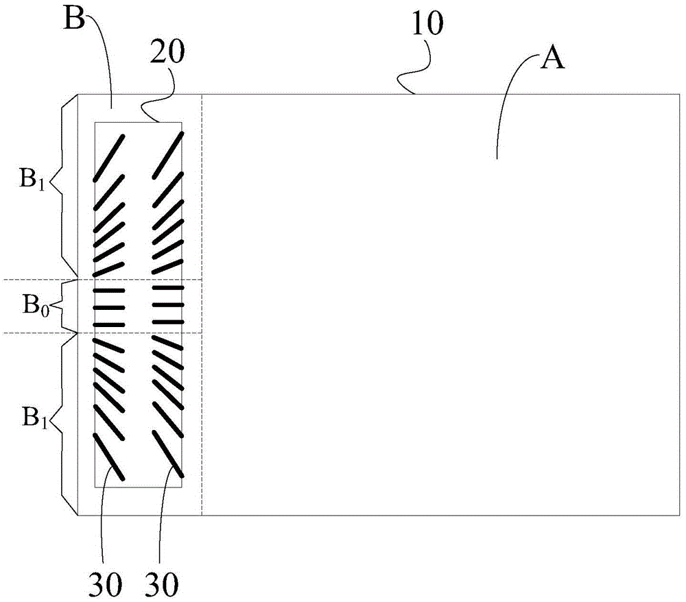
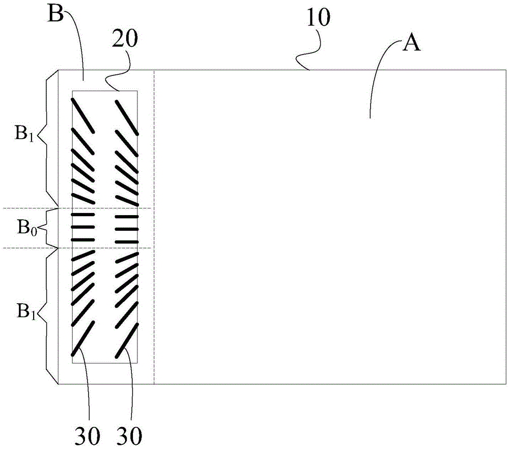
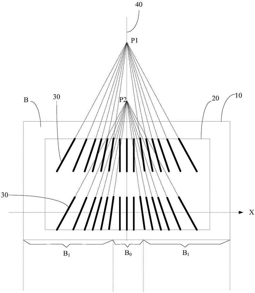
[0042] A display device provided by an embodiment of the present invention, such as Figure 1a with Figure 1b As shown, it includes a flexible display panel 10 and a chip 20 bonded to the non-display area B of the flexible display panel 10, wherein the chip 20 is on the side close to the display area A of the flexible display panel 10 and on the side away from the display area A, respectively. There are a plurality of mutually independent pins 30 in ...


PUM


Abstract

The invention discloses a display device and a chip binding method thereof. The display device comprises a flexible display panel and a chip bound on a non-display region of the flexible display panel. Due to the fact that extension directions of all pins meet the following condition that in each row of pins, at least the pins located on the side region are converged on the same point in a datum line along extension lines at the same end according to the regions of the pins, and the included angles between respective extension lines of the two pins belonging to the same pin set and the datum line are equal. Thus, when the size of the flexible display panel is changed in the first direction, the flexible display panel and the chip can be bound after the relative positions, perpendicular to the first direction, of the flexible display panel and the chip are adjusted, and therefore it is guaranteed that correct alignment of the pins of the chip and the pins of the flexible display panel can be achieved as long as the size change of the flexible display panel in the first direction is within a certain range, and the chip binding yield of the display device is increased.

Description

technical field [0001] The invention relates to the field of display technology, in particular to a display device and a chip bonding method thereof. Background technique [0002] Permanent display technology is a research hotspot in the field of display technology in recent years. Because of its advantages of being thinner, more shock-resistant, and lighter, it will be widely used in civilian and military fields. Flexible display can be defined as the substrate of the display panel made of a very thin flexible substrate, which can be bent to a radius of curvature of only a few centimeters or less without damaging the display function of the display panel. [0003] When making a flexible display device, the flexible substrate is generally fixed on the glass substrate first, and then the subsequent flexible display panel manufacturing process is performed. This process is compatible with the existing display panel manufacturing equipment. After the flexible display panel is m...

Claims


Application Information

Patent Timeline
IPC IPC(8): G09F9/30
CPCG09F9/301H01L23/48H01L23/528G09G2380/02H01L24/16H01L24/81H01L2223/54486H01L2224/1412H01L2224/16225H01L2224/81201H01L2224/13012H01L2224/81125H01L2224/81127H01L23/544H05K2201/10128H01L24/13H01L24/14H05K1/11G09G3/20H01L21/77H01L27/12H01L2224/11H01L2224/12H05K13/046
Inventor 陈立强李红
Owner BOE TECH GRP CO LTD
Why Eureka
Try Eureka