
Low-temperature wafer direct bonding machine and wafer bonding method

A direct bonding and wafer bonding technology, which is applied in the fields of electrical components, semiconductor/solid-state device manufacturing, circuits, etc., can solve problems such as poor debonding and synthesis efficiency, and achieve the goals of avoiding scrapping, improving success rate, and improving efficiency Effect

Active Publication Date: 2019-08-06
ICLEAGUE TECH CO LTD
View PDF6 Cites 9 Cited by
  • Summary
  • Abstract
  • Description
  • Claims
  • Application Information

AI Technical Summary

Problems solved by technology

[0005] However, the existing debonding technology still has the problem of poor success rate of debonding

Method used


Image

  • Low-temperature wafer direct bonding machine and wafer bonding method
  • Low-temperature wafer direct bonding machine and wafer bonding method
  • Low-temperature wafer direct bonding machine and wafer bonding method

Examples


Embodiment Construction

[0037] As mentioned in the background art, the existing debonding technology still has the problem of poor success rate of debonding.

[0038] The study found that although debonding technology can be used to separate pre-bonded wafer pairs, the success rate of separation depends on time (the time between pre-bonding and debonding), and the longer the time, the lower the success rate of debonding (Unless all factors are perfectly controlled, the success rate is <=70%), because the bonding strength between the pre-bonded wafer pair has an absolute relationship with the time of placement, at room temperature, the pre-bonded wafer The bonding strength of the pair will increase rapidly in a short period of time, and the increase in bonding strength will lead to a decrease in the success rate of debonding.

[0039] Moreover, the existing low-temperature wafer bonding generally includes four processes of surface treatment, pre-bonding, missing detection, and annealing. It is carried ...


PUM


Abstract

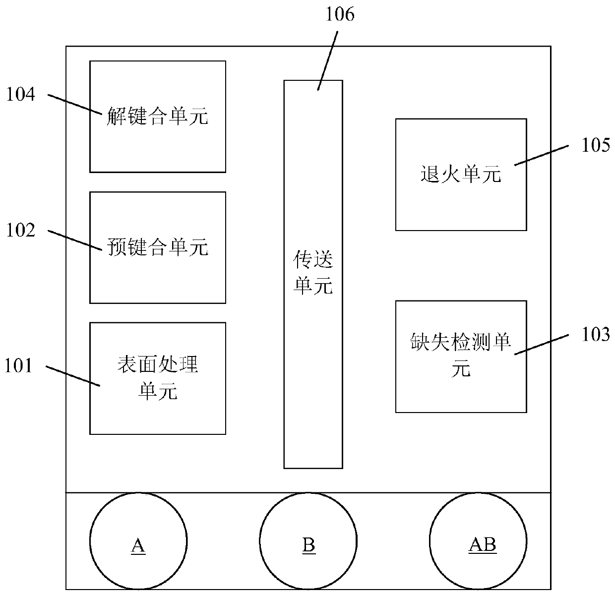
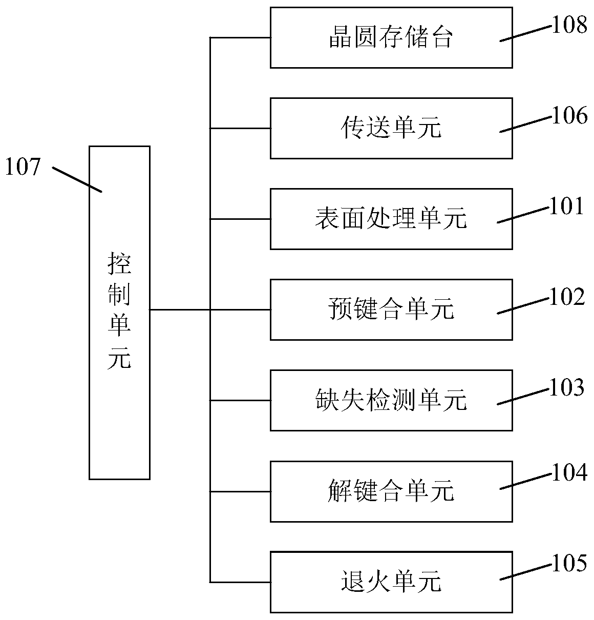
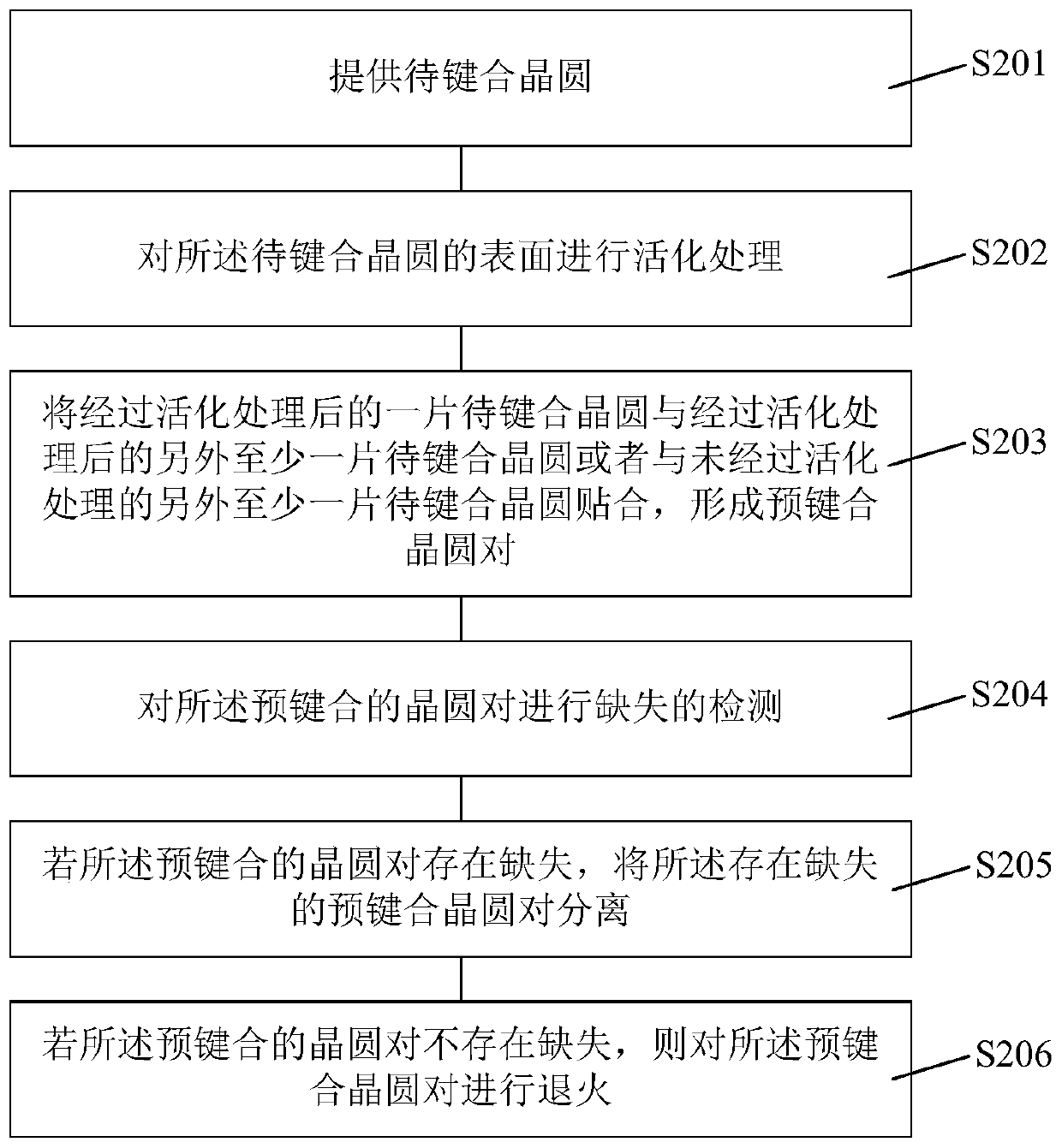
A low-temperature wafer bonding machine and a wafer bonding method are provided. The low-temperature wafer bonding machine comprises a surface treatment unit used for activating the surfaces of to-be-bonded wafers, a pre-bonding unit used for bonding one activated to-be-bonded wafer to at least one other activated to-be-bonded wafer or at least one other unactivated to-be-bonded wafer to form a pre-bonded wafer pair, a missing detection unit used for detecting whether the pre-bonded wafer pair is missing, and a de-bonding unit used for separating the missing pre-bonded wafer pair. The successrate of de-bonding of the low-temperature wafer bonding machine of the invention is improved.

Description

technical field [0001] The invention relates to the field of wafer bonding, in particular to a low-temperature wafer direct bonding machine and a wafer bonding method. Background technique [0002] Low-temperature wafer direct bonding technology is the most popular bonding method in recent years, and it is also the most difficult bonding method that has the highest requirements on the surface morphology and surface treatment process of silicon wafers. The process of wafer direct bonding has experienced from the early high-temperature bonding (melting point of silicon, about 1410°C) to the low-temperature wafer bonding process (room temperature pre-bonding plus low-temperature annealing (general annealing temperature ≤410℃)), mainly to overcome the influence of high temperature on devices, so people began to pay attention to the research of low temperature wafer bonding. [0003] At present, the main researches on low temperature wafer bonding include hydrophilic bonding and...

Claims


Application Information

Patent Timeline
Patent Type & Authority Applications(China)
IPC IPC(8): H01L21/67H01L21/66H01L21/18
CPCH01L21/187H01L21/67092H01L21/67253H01L21/67288H01L22/12H01L22/20
Inventor 周华
Owner ICLEAGUE TECH CO LTD
Learn More