Light emitting diode package structure

Inactive Publication Date: 2010-06-17
EVERLIGHT ELECTRONICS
View PDF3 Cites 10 Cited by
  • Summary
  • Abstract
  • Description
  • Claims
  • Application Information

AI Technical Summary

Benefits of technology

[0009]The present invention provides an LED package struct

Problems solved by technology

However, during the movement of the bonding tip B, it is easy for the bonding tip B to hit the spacer 146 protruding from the surface 112, which leads to the

Method used


Image

  • Light emitting diode package structure
  • Light emitting diode package structure
  • Light emitting diode package structure

Examples


Embodiment Construction

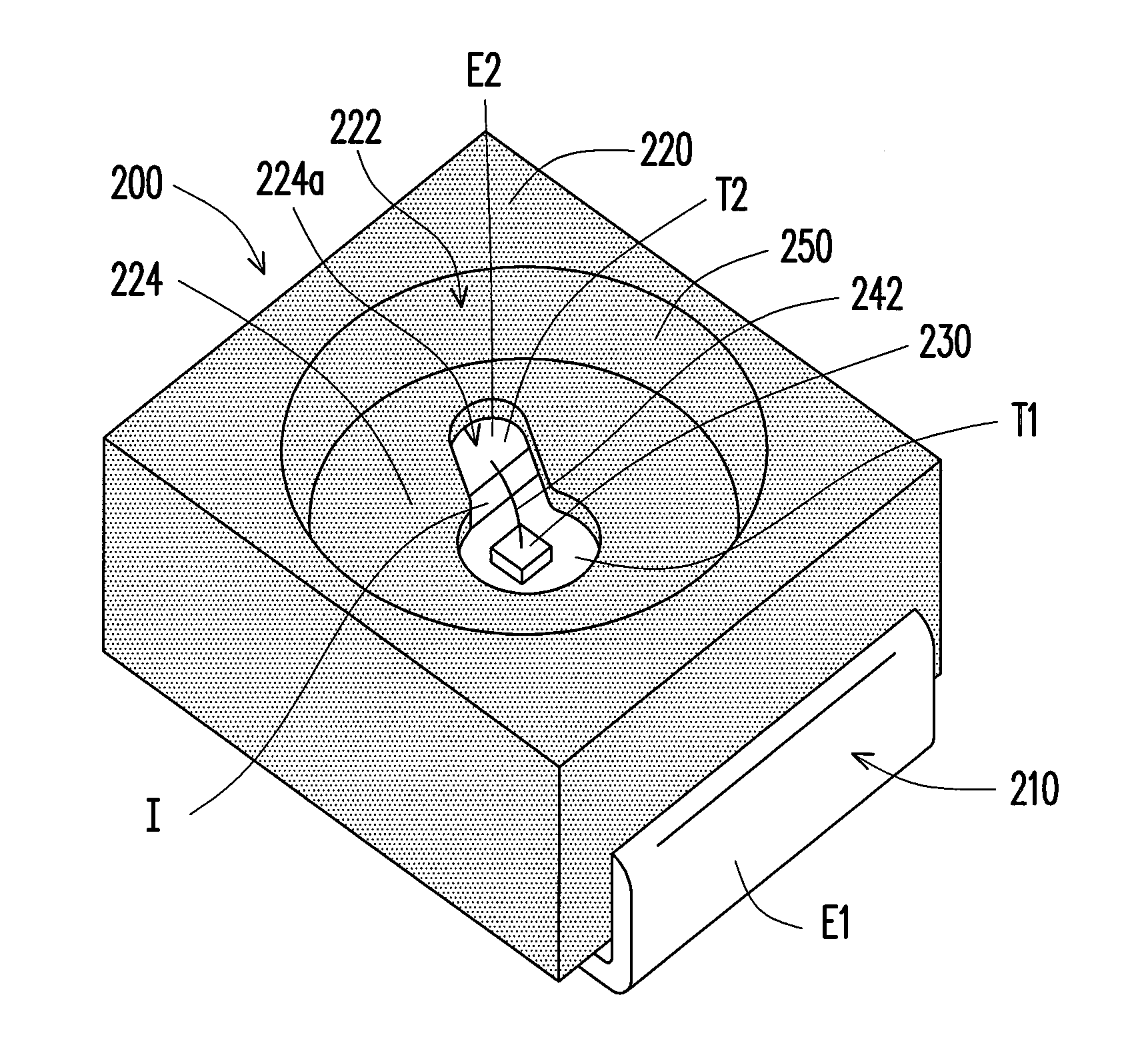
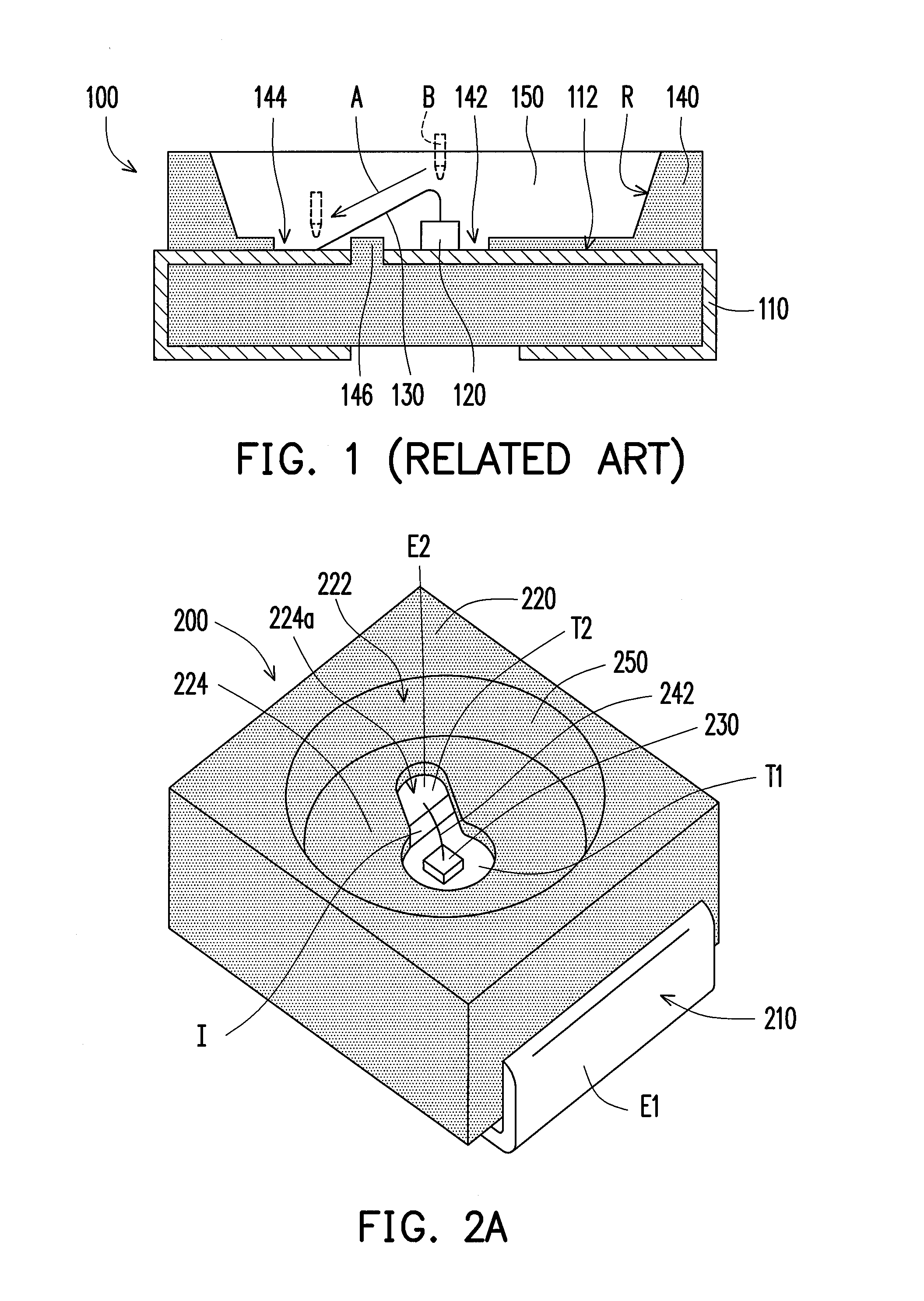
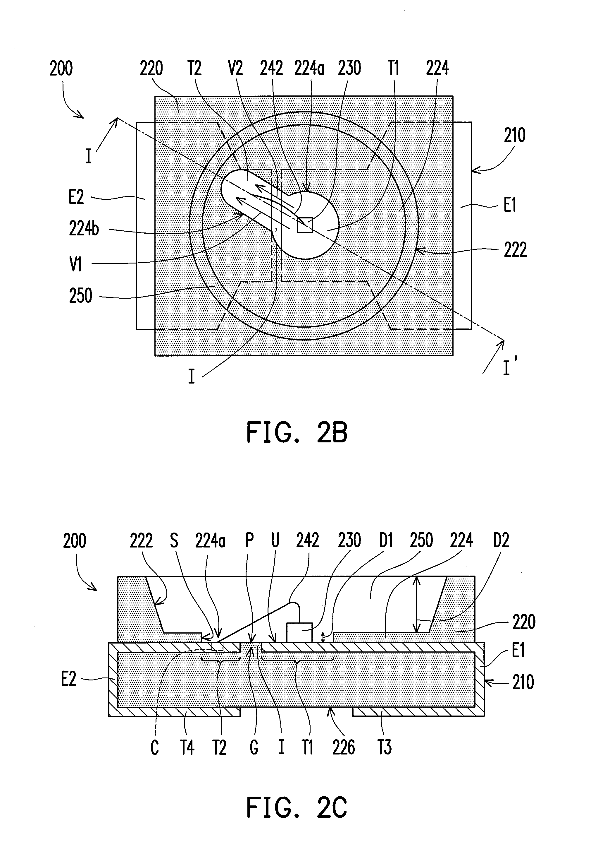
[0033]FIG. 2A is a schematic view illustrating an LED package structure according to one embodiment of the present invention, FIG. 2B is a schematic top view of the LED package structure in FIG. 2A and FIG. 2C is a schematic cross-sectional view along line I-I′ of the LED package structure in FIG. 2B.

[0034]As shown in FIG. 2A together with FIG. 2B and FIG. 2C, a light emitting diode (LED) package structure 200 comprises a lead frame 210, a housing 220, an LED chip 230, a first wire 242 and a light-transmissive encapsulant 250. The leadframe 210 has a first electrode E1 and a second electrode E2 separated from each other.

[0035]The housing 220 wraps a portion of the leadframe 210. In other words, the portion of the leadframe 210 is configured in the housing 220. Specifically, in the present embodiment, a third end T3 of the first electrode E1 and a fourth end T4 of the second electrode E2 respectively outwardly extend from an inner surface of the housing 220 toward a bottom surface 22...


PUM


Abstract

A light emitting diode (LED) package structure including a leadframe, a housing, a LED chip and a light-transmissive encapsulant is provided. The leadframe has a first electrode and a second electrode separated from each other. The housing wraps the first electrode and the second electrode and includes a recess having a bottom and a sidewall. The bottom of the recess has a cover layer covering the leadframe and having an opening exposing an end of the first electrode, an end of the second electrode and a spacer disposed therebetween and connected thereto wherein the spacer, the end of the first electrode and the end of the second electrode are substantially coplanar. The LED chip is disposed in the recess and electrically connected to leadframe. The light-transmissive encapsulant is filled in the recess.

Description

CROSS-REFERENCE TO RELATED APPLICATION[0001]This application claims the priority benefit of Taiwan applications serial no. 97222510 and 98135965, filed on Dec. 15, 2008 and Oct. 23, 2009. The entirety of each of the above-mentioned patent applications is hereby incorporated by reference herein and made a part of this specification.BACKGROUND OF THE INVENTION[0002]1. Field of the Invention[0003]The present invention generally relates to a package structure, and particularly to a light-emitting diode package structure.[0004]2. Description of Related Art[0005]The light-emitting diode has the advantages including low power consumption, long device lifetime, no idling time and fast response speed. Besides, the LED has the features of small dimension, great resistance to vibration, capability for mass production and easily to be adapted to the ultra-small or array device under demand so that the LED is widely used on the indicator or display device of the information appliance, the teleco...

Claims


Application Information

Patent Timeline
IPC IPC(8): H01L33/62
CPCH01L33/486H01L33/60H01L33/62H01L2224/48091H01L2224/48247H01L2224/78301H01L2924/00014
Inventor SHEU, SHENG-JIAHSU, CHIH-HUNGHSIEH, CHUNG-CHUAN
Owner EVERLIGHT ELECTRONICS
Why Eureka
Try Eureka