Enhanced high electronic mobility transistor and manufacturing method thereof

A high electron mobility, transistor technology, applied in semiconductor/solid-state device manufacturing, circuits, electrical components, etc., can solve the problem of high interface state density in the dielectric layer, improve breakdown voltage and power performance, and reduce material damage and defects , Reduce the effect of current collapse effect

Active Publication Date: 2016-06-08
GPOWER SEMICON
View PDF8 Cites 20 Cited by
  • Summary
  • Abstract
  • Description
  • Claims
  • Application Information

AI Technical Summary

Problems solved by technology

[0007] The present invention is completed in order to solve the above-mentioned deficiencies in the prior art. The purpose of the present invention is to provide an enhanced high electron mobility transistor and its manufacturing method, which can solve the problem of high interface state density of the dielectric layer in the prior art. problem, and at the same time implement the enhanced

Method used


Image

  • Enhanced high electronic mobility transistor and manufacturing method thereof
  • Enhanced high electronic mobility transistor and manufacturing method thereof
  • Enhanced high electronic mobility transistor and manufacturing method thereof

Examples


Embodiment 1

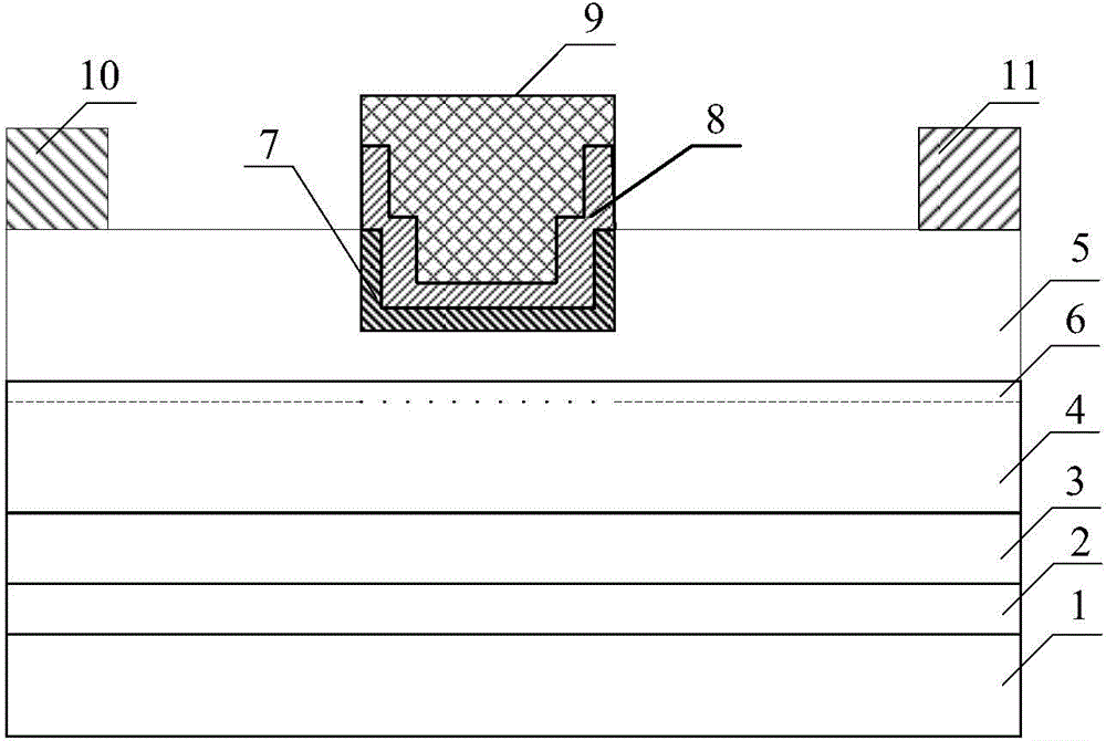
[0054] figure 1 It is a structural diagram of an enhancement-mode high electron mobility transistor provided in Embodiment 1 of the present invention. Such as figure 1 As shown, the enhanced high electron mobility transistor provided by Embodiment 1 of the present invention includes:

[0055] Substrate 1.

[0056] In this embodiment, the substrate material may be silicon, gallium nitride, silicon carbide or sapphire.

[0057] The nucleation layer 2 is located on the substrate 1 .

[0058] In this embodiment, the material of the nucleation layer may be aluminum nitride, gallium nitride or other III-V group compounds.

[0059] The buffer layer 3 is located on the nucleation layer 2 .

[0060] In this embodiment, the material of the buffer layer may be AlGaN or other III-V compounds.

[0061] The channel layer 4 is located on the buffer layer 3 .

[0062] In this embodiment, the material of the channel layer may be gallium nitride or other III-V compounds.

[0063] The ba...

Embodiment 2

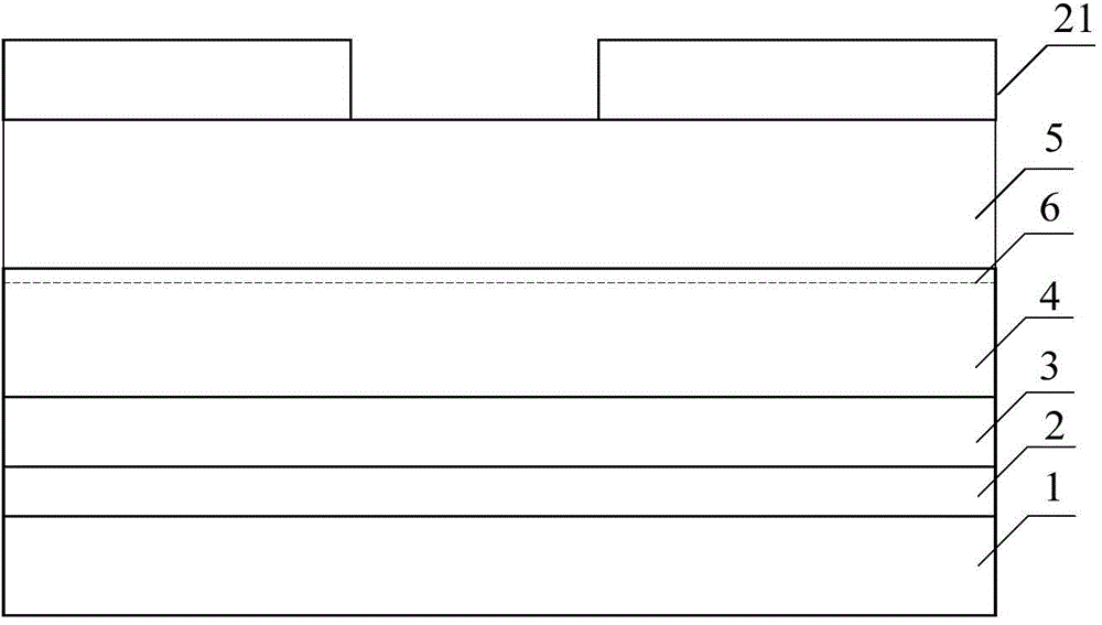
[0100] image 3 It is a structural diagram of the enhanced high electron mobility transistor provided in Embodiment 2 of the present invention. Such as image 3 As shown, the difference from the first embodiment of the present invention is that in the enhanced high electron mobility transistor provided by the second embodiment of the present invention, the secondary grown semiconductor epitaxial layer 7 expands toward the drain 11, and a junction termination structure is introduced, when When the Al composition in the secondary grown semiconductor epitaxial layer 7 is smaller than the Al composition in the barrier layer 5, it will have a certain depletion effect on the two-dimensional electron gas under the junction terminal, thereby reducing the The electric field spike increases the breakdown voltage of the device.

[0101] The manufacturing method of the enhanced high electron mobility transistor provided in the second embodiment of the present invention includes the foll...

Embodiment 3

[0123] Figure 5 It is a structural diagram of the enhanced high electron mobility transistor provided in Embodiment 3 of the present invention. Such as Figure 5 As shown, different from the second embodiment of the present invention, the enhanced high electron mobility transistor provided by the third embodiment of the present invention further includes: an in-situ mask layer 12 located on the barrier layer 5, an in-situ dielectric layer 8 It is located on the secondary grown semiconductor epitaxial layer 7 and the in-situ mask layer 12 .

[0124] In this embodiment, the in-situ mask layer is obtained by in-situ growth on the barrier layer by using the same preparation method without taking the wafer out of the growth chamber after the growth of the barrier layer is completed. This preparation method can obtain an in-situ mask layer with better crystal quality, and effectively reduce the interface state between the mask layer and the potential barrier layer.

[0125] Wher...


PUM


Abstract

The invention discloses an enhanced high electronic mobility transistor and a manufacturing method thereof. The transistor comprises a substrate, a channel layer located above the substrate, a barrier layer located on the channel layer, a groove located in the barrier layer; a secondary growth semiconductor epitaxial layer located on the groove, an orthotopic dielectric layer located on the secondary growth semiconductor epitaxial layer, a grid electrode located on the orthotopic dielectric layer, a source electrode located on the barrier layer and a drain electrode located on the barrier layer, wherein a two-dimensional electron gas is formed at an interface position of the barrier layer and the channel layer. By using the enhanced high electronic mobility transistor, material damages and defects caused by etching can be reduced, an interface state density of the groove and the secondary growth semiconductor epitaxial layer and an interface state density of the orthotopic dielectric layer and the secondary growth semiconductor epitaxial layer are decreased, electric leakage of the grid electrode is reduced, a breakdown voltage and power performance of the transistor are increased and a degradation effect of a dynamic conduction resistor is reduced.

Description

technical field [0001] The invention relates to the technical field of semiconductors, in particular to an enhanced high electron mobility transistor and a manufacturing method thereof. Background technique [0002] The third-generation wide-bandgap semiconductor materials represented by GaN (gallium nitride) have excellent properties such as wide bandgap, high breakdown electric field strength, high saturation electron drift velocity, high thermal conductivity, and high concentration of two-dimensional electron gas at the heterogeneous interface. Compared with Si (silicon) materials, GaN is more suitable for making power electronic devices with high power, high voltage and high switching speed. Compared with traditional Si devices, GaN devices can carry higher power density and have higher energy conversion efficiency, which can reduce the volume and weight of the entire system, thereby reducing system cost. [0003] At present, a large part of research is only aimed at de...

Claims


Application Information

Patent Timeline
Patent Type & Authority Applications(China)
IPC IPC(8): H01L29/778H01L21/335H01L29/06
CPCH01L29/4236H01L29/7786H01L29/2003H01L29/66462
Inventor 裴轶
Owner GPOWER SEMICON
Why Eureka
Try Eureka