Touch scanning circuit, driving method thereof, touch driving circuit and touch display screen

A technology of touch scanning and circuit, which is applied in the field of touch scanning circuit, touch driving circuit and touch display screen, and can solve the problems of restricting the application of embedded technology, increasing the number of lines, and increasing the wiring space

Active Publication Date: 2016-06-15
BOE TECH GRP CO LTD +1
View PDF3 Cites 4 Cited by
  • Summary
  • Abstract
  • Description
  • Claims
  • Application Information

AI Technical Summary

Problems solved by technology

However, as the size of the display screen increases and the number of touch scanning lines Txn increases, the wiring for transmitting touch scanning signals to the touch scanning line Txn also increases accordingly, resulting in an increase in the space occupied by the wiring. , thus limiting the application of in-cell technology on large-size and narrow-frame displays

Method used


Image

  • Touch scanning circuit, driving method thereof, touch driving circuit and touch display screen
  • Touch scanning circuit, driving method thereof, touch driving circuit and touch display screen
  • Touch scanning circuit, driving method thereof, touch driving circuit and touch display screen

Examples


example 1

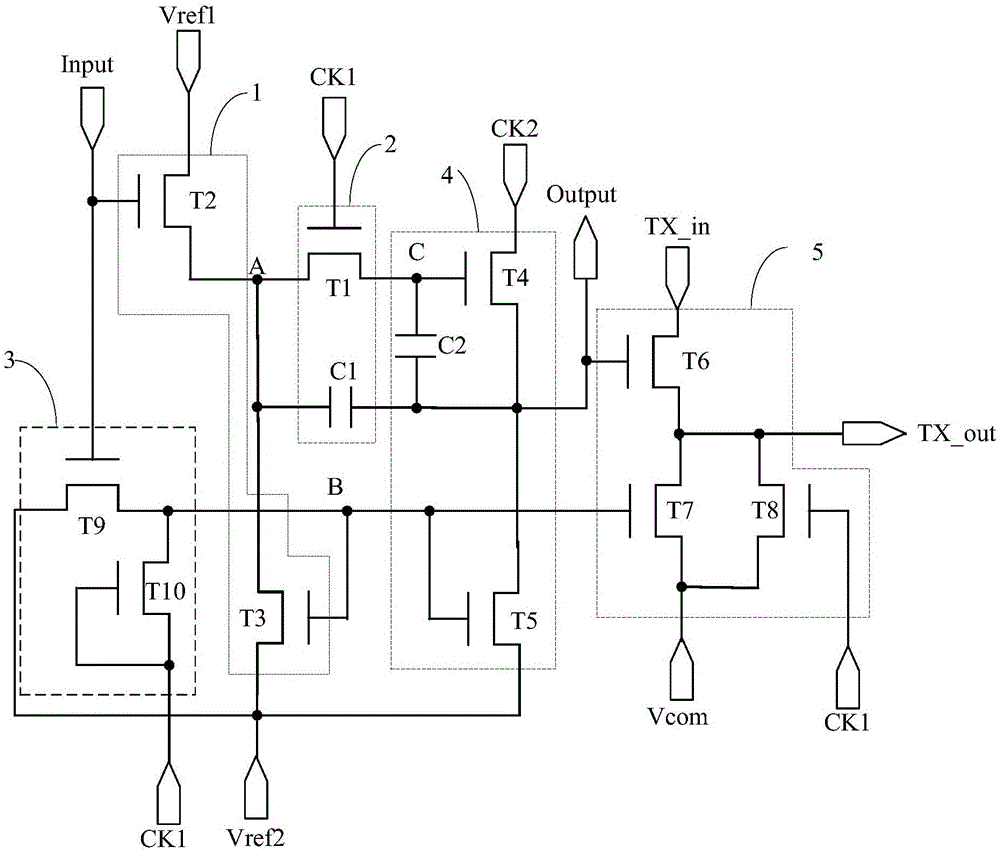
[0115] Figure 3a Take the touch scanning circuit shown as an example, and the corresponding input and output timing diagram is as follows Figure 5a shown. Specifically, choose the Figure 5a The four stages of T1 ~ T4 in the input and output sequence diagram shown.

[0116] In the T1 stage: Input=1, CK1=1, CK2=0.

[0117] Because Input=1, the second switch transistor T2 and the ninth switch transistor T9 are turned on, and because CK1=1, the first switch transistor T1, the tenth switch transistor T10 and the eighth switch transistor T8 are turned on; the second reference signal terminal Vref2 The low-potential signal of the first clock signal terminal CK1 is provided to the second node B through the turned-on ninth switch transistor T9, and the high-potential signal of the first clock signal terminal CK1 is provided to the second node B through the turned-on tenth switch transistor T10, so the second Node B is low potential, and the second node B of low potential control...

example 2

[0127] Figure 3b Take the touch scanning circuit shown as an example, and the corresponding input and output timing diagram is as follows Figure 5b shown. Specifically, choose the Figure 5b The four stages of T1 ~ T4 in the input and output sequence diagram shown.

[0128] In the T1 stage: Input=1, CK1=1, CK2=0.

[0129] Since Input=1, the second switch transistor T2 and the eleventh switch transistor T11 are turned on, and because CK1=1, the first switch transistor T1 and the eighth switch transistor T8 are turned on; the low potential signal of the second reference signal terminal Vref2 passes through The turned-on eleventh switching transistor T11 is provided to the second node B, and at the same time, the first clock signal terminal CK1 starts to charge the third capacitor C3, the potential of the second node B is a low potential, and the low potential second node B controls the second node B The three switching transistors T3, the fifth switching transistor T5 and ...

example 3

[0139] Figure 3c Take the touch scanning circuit shown as an example, and the corresponding input and output timing diagram is as follows Figure 5a shown. Specifically, choose the Figure 5a The four stages of T1 ~ T4 in the input and output sequence diagram shown.

[0140] In the T1 stage: Input=1, CK1=1, CK2=0.

[0141] Since Input=1, the second switching transistor T2, the twelfth switching transistor T12 and the thirteenth switching transistor T13 are turned on, and since CK1=1, the first switching transistor T1, the fourteenth switching transistor T14 and the eighth switching transistor T8 conduction; the low potential signal of the second reference signal terminal Vref2 is provided to the gate of the fifteenth switching transistor T15 through the turned-on twelfth switch transistor T12; the low potential signal of the second reference signal terminal Vref2 is passed through the turned-on first The thirteenth switch transistor T13 is provided to the second node B; a...


PUM


Abstract

The invention discloses a touch scanning circuit, a driving method thereof, a touch driving circuit and a touch display screen. The touch scanning circuit comprises an input unit, a first control unit, a second control unit, a displacement output unit and a touch output unit; wherein the input unit is used for controlling the potential of a first node; the first control unit is used for controlling on and off between the first node and a third node; the second control unit is used for controlling the potential of a second node; the displacement output unit is used for controlling the potentialof a displacement output end according to the third node and the second node; the control output unit is used for controlling signals output by a touch output end according to the second node, the touch output end and a first clock signal end. The touch scanning circuit in a simple structure is realized by the aid of the matching of the five units.

Description

technical field [0001] The invention relates to the field of touch technology, in particular to a touch scanning circuit, a driving method thereof, a touch driving circuit and a touch display screen. Background technique [0002] With the rapid development of display technology, touch screens (TouchScreenPanel) have gradually spread in people's lives. At present, touch screens can be divided into three types according to their composition structures: Add-on Mode Touch Panel, OnCell Touch Panel, and InCell Touch Panel. Among them, the plug-in touch screen is produced separately from the touch screen and the display screen, and then bonded together to form a display screen with touch function. The plug-in touch screen has disadvantages such as high production cost, low light transmittance, and thick modules. The embedded touch screen embeds the touch electrodes of the touch screen inside the display screen, which can reduce the overall thickness of the module and greatly redu...

Claims


Application Information

Patent Timeline
Patent Type & Authority Applications(China)
IPC IPC(8): G06F3/041G06F3/044
CPCG06F3/0412G06F3/044G06F3/04166G06F3/04184G06F2203/04112G09G2310/0264G06F3/04164
Inventor 谭文邓银韦东梅
Owner BOE TECH GRP CO LTD
Why Eureka
Try Eureka