Surface-plasma-enhanced two-dimensional material/semiconductor heterojunction solar cell and preparation method therefor

A surface plasmon and solar cell technology, applied in semiconductor devices, nanotechnology for materials and surface science, circuits, etc., can solve the problems of high cost of solar cell power generation, high cost of battery manufacturing, low photoelectric conversion efficiency, etc., to achieve Ease of promotion, improvement of conversion efficiency, and remarkable effect

Active Publication Date: 2016-06-15
ZHEJIANG UNIV
View PDF2 Cites 27 Cited by
  • Summary
  • Abstract
  • Description
  • Claims
  • Application Information

AI Technical Summary

Benefits of technology

The technical effect of this patented technology involves improving the performance of photovoltaic devices by utilizing direct interaction between light waves or electromagnetic radiation (EM) near surfaces called surface Plasmons (SPs). This results from enhanced electric fields at certain areas within these materials due to localized high levels of charge density caused by quantum interference phenomena such as electron transfer reactions during photoexcitation process. By focusing strong laser beams onto specific regions where SPs are found, it becomes possible for more efficient energy production without adding complexity into existing manufacturing methods.

Problems solved by technology

The technical problem addressed by this patented technology relates to improving the performance of photovoltaic devices made from different types of nanoparticles (NP) due to their low production costs while also enhancing their ability to convert sunlight into electrical or other forms of useful work without losing too much weight during use.

Method used


Image

  • Surface-plasma-enhanced two-dimensional material/semiconductor heterojunction solar cell and preparation method therefor
  • Surface-plasma-enhanced two-dimensional material/semiconductor heterojunction solar cell and preparation method therefor

Examples


Embodiment 1

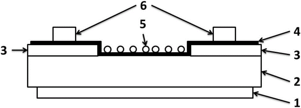
[0023] 1) Using thermal evaporation to deposit chromium-gold composite electrode on the back of n-type gallium arsenide;

[0024] 2) On the other side of the gallium arsenide substrate, a 100 nm thick aluminum oxide electrode insulating layer is deposited by electron beam evaporation and a mask method;

[0025] 3) Transfer 0.4 nanometer thick graphene to the side of the gallium arsenide substrate with the electrode insulating layer using PMMA as a support layer and cover part of the graphene on the aluminum oxide electrode insulating layer;

[0026] 4) Coat the silver paste directly on the graphene within the electrode insulating layer and dry it as the front electrode;

[0027] 5) Spin-coating 80 nanometers of gold quantum dot solution on graphene to obtain a surface plasma enhanced graphene / gallium arsenide heterojunction solar cell.

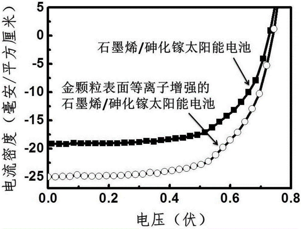
[0028] The obtained surface plasma-enhanced graphene / gallium arsenide heterojunction solar cell produces a local field enhancement on the surface of th...

Embodiment 2

[0030] 1) Using thermal evaporation to deposit titanium-silver composite electrode on the back of n-type silicon;

[0031] 2) Using plasma enhanced chemical vapor deposition and a mask method to deposit a silicon nitride electrode insulating layer with a thickness of 200 microns on the other side of the silicon substrate;

[0032] 3) Transfer the 500-nm-thick molybdenum disulfide to the side of the silicon substrate with the electrode insulating layer using PMMA as a support layer and cover part of the molybdenum disulfide on the silicon nitride electrode insulating layer;

[0033] 4) Magnetron sputtering is used to deposit nickel on the molybdenum disulfide in the range of the electrode insulating layer as the front electrode;

[0034] 5) Spin-coating a silver quantum dot solution with a particle diameter of 200 nanometers on graphene to obtain a surface plasma enhanced molybdenum disulfide / silicon heterojunction solar cell.

Embodiment 3

[0036] 1) Using thermal evaporation to deposit a copper-platinum composite electrode on the back of p-type indium phosphide;

[0037] 2) Depositing a 2nm thick titanium oxide electrode insulating layer on the other side of the indium phosphide substrate by atomic layer deposition and masking;

[0038] 3) Transfer the 20-nanometer-thick tungsten disulfide to the side of the indium phosphide substrate with the electrode insulating layer using PMMA as a support layer and cover part of the tungsten disulfide on the aluminum oxide electrode insulating layer;

[0039] 4) Print silver paste on the tungsten disulfide in the range of the electrode insulating layer and dry it as the front electrode;

[0040] 5) Spin-coating a 5 nanometer particle diameter aluminum quantum dot solution on graphene to obtain a surface plasma enhanced tungsten disulfide / indium phosphide heterojunction solar cell.


PUM

PropertyMeasurementUnit
Thicknessaaaaaaaaaa
Thicknessaaaaaaaaaa
Sizeaaaaaaaaaa

Abstract

The invention discloses a surface-plasma-enhanced two-dimensional material/semiconductor heterojunction solar cell and a preparation method therefor. The solar cell is provided with a back surface electrode, a semiconductor substrate, a two-dimensional material and a metal quantum dot layer from the bottom up in sequence, wherein a front surface electrode is also arranged on the two-dimensional layer; an electrode insulating layer is arranged between the semiconductor substrate and the two-dimensional layer; the preparation method comprises the steps of manufacturing the back surface electrode on one surface of the semiconductor substrate, and then manufacturing the electrode insulating layer on the other surface of the semiconductor substrate; moving the two-dimensional material to the semiconductor substrate; and manufacturing the metal quantum dot layer and the front surface electrode on the two-dimensional material. According to the surface-plasma-enhanced two-dimensional material/semiconductor heterojunction solar cell, the surface plasma resonance is utilized to improve the conversion efficiency of the two-dimensional material/semiconductor heterojunction solar cell; and meanwhile, the solar cell is simple in process and convenient to popularize.

Description


Claims


Application Information

Patent Timeline
Owner ZHEJIANG UNIV
Why Eureka
Try Eureka