Organic electroluminescent device and display device

An electroluminescence device and electroluminescence technology, which are applied in the directions of organic semiconductor devices, electro-solid devices, electrical components, etc., can solve the problems of high driving voltage, low power consumption efficiency, and high power consumption, and improve current efficiency and power. Efficiency, the effect of reducing the driving voltage

Inactive Publication Date: 2016-06-15
TCL CHINA STAR OPTOELECTRONICS TECH CO LTD
View PDF6 Cites 0 Cited by
  • Summary
  • Abstract
  • Description
  • Claims
  • Application Information

AI Technical Summary

Problems solved by technology

However, the color purity and color rendering of the formed white light are low, and because the carriers at each interface cannot be effectively separated, resulting in unbalanced carrier injection and recombination in the blue light emitting material layer and the yellow light emitting material layer, The current efficiency of the WOLED device is low, and the driving voltage is high, resulting in low power consumption efficiency and high power consumption.

Method used


Image

  • Organic electroluminescent device and display device
  • Organic electroluminescent device and display device
  • Organic electroluminescent device and display device

Examples


Embodiment Construction

[0019] The following will clearly and completely describe the technical solutions in the embodiments of the present invention with reference to the accompanying drawings in the embodiments of the present invention. Obviously, the described embodiments are only some of the embodiments of the present invention, not all of them. Based on the embodiments of the present invention, all other embodiments obtained by persons of ordinary skill in the art without making creative efforts belong to the protection scope of the present invention.

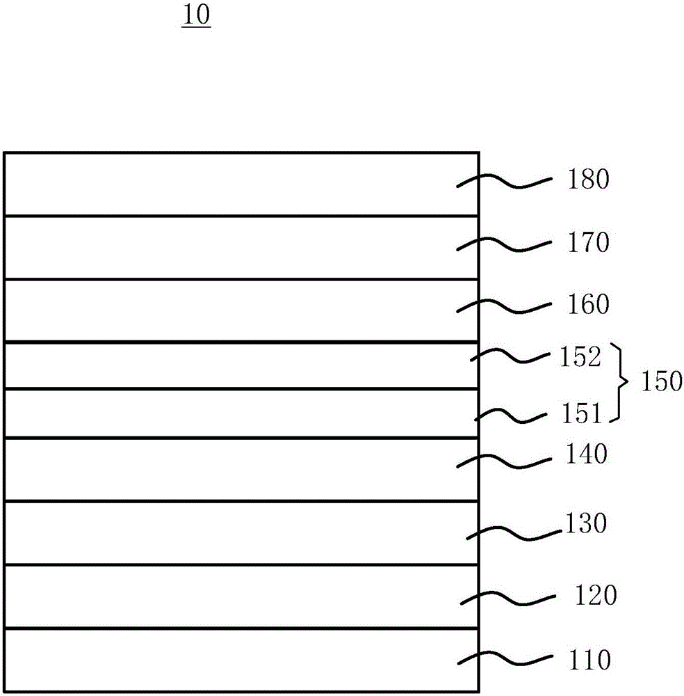
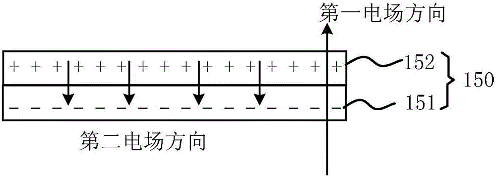
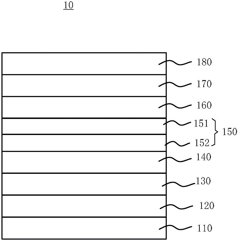
[0020] Please also refer to figure 1 and figure 2 , figure 1 It is a schematic cross-sectional structure diagram of an organic electroluminescent device in a preferred embodiment of the present invention; figure 2 It is a schematic diagram of the direction of the electric field in the heterojunction and the electric field in the organic electroluminescence device in the present invention. The organic electroluminescent device 10 may be, but ...


PUM


Abstract

The invention provides an organic electroluminescent device and a display device. The organic electroluminescent device comprises a substrate, a first electrode, a first type carrier transmission and injection layer, a first light-emitting layer, a hetero-junction, a second light-emitting layer, a second type carrier transmission and injection layer and a second electrode, wherein the first electrode, the first type carrier transmission and injection layer, the first light-emitting layer, the hetero-junction, the second light-emitting layer, the second type carrier transmission and injection layer and the second electrode are stacked up at the same side of the substrate in sequence. The first electrode provides first type carriers, which are then transmitted to the first light-emitting layer through the first type carrier transmission and injection layer; the second electrode provides second type carriers, which are then transmitted to the second light-emitting layer through the second type carrier transmission and injection layer; the hetero-junction generates excitons, which are separated into the first type carriers and second type carriers; the first type carriers of the first electrode and the second type carriers in the hetero-junction are compounded in the first light-emitting layer to generate first light rays; the second type carriers of the second electrode and the first type carriers in the hetero-junction are compounded in the second light-emitting layer to generate second light rays; and the first light rays and the second light rays are mixed to form white light.

Description

technical field [0001] The invention relates to the display field, in particular to an organic electroluminescence device and a display device. Background technique [0002] Organic electroluminescent devices, such as organic light emitting diodes (Organic Light Emitting Diode, OLED), have attracted extensive attention in the industry due to their own advantages such as self-illumination, fast response speed, wide viewing angle, thinness, and low power consumption. It is of great significance to realize that a white organic light emitting diode (WhiteOrganicLightEmittingDiode, WOLED) can be used as a light source in the lighting field, and a full-color display can be realized by adding a color filter to the WOLED and applied in the display field. At present, WOLED is mainly formed by binary complementary colors or three primary colors. The binary complementary color WOLED mainly introduces a stacked structure of a blue light-emitting material layer and a yellow light-emitti...

Claims


Application Information

Patent Timeline
Patent Type & Authority Applications(China)
IPC IPC(8): H01L51/50H01L51/52H01L27/32
CPCH10K59/00H10K50/14H10K50/17H10K50/80H10K50/00H10K50/131H10K50/13H10K50/15H10K50/16H10K50/81H10K50/82H10K50/171H10K59/30
Inventor 周凯锋
Owner TCL CHINA STAR OPTOELECTRONICS TECH CO LTD
Why Eureka
Try Eureka