Supercharge Your Innovation With Domain-Expert AI Agents!

Local bump epitaxy for improved contact by local silicon capping during trench silicide processing

A technology of contacts and epitaxial materials, applied in the direction of semiconductor/solid-state device parts, semiconductor devices, electrical components, etc.

Active Publication Date: 2019-07-02
GLOBALFOUNDRIES INC
View PDF3 Cites 0 Cited by
  • Summary
  • Abstract
  • Description
  • Claims
  • Application Information

AI Technical Summary

Problems solved by technology

However, silicidation of unmerged source-drains introduces new defects

Method used


Image

  • Local bump epitaxy for improved contact by local silicon capping during trench silicide processing
  • Local bump epitaxy for improved contact by local silicon capping during trench silicide processing
  • Local bump epitaxy for improved contact by local silicon capping during trench silicide processing

Examples


Embodiment Construction

[0021] As noted above, the present disclosure relates to finFET structures with low source / drain contact resistance and methods of fabrication thereof. Aspects of the present disclosure will now be described in detail with reference to the accompanying drawings. It should be noted that the same reference numerals refer to the same elements for different embodiments. The drawings are not necessarily drawn to scale. As used herein, ordinal numbers such as "first" and "second" are used only to distinguish similar elements, and different ordinal words may be used to refer to the same elements in the specification and / or claims.

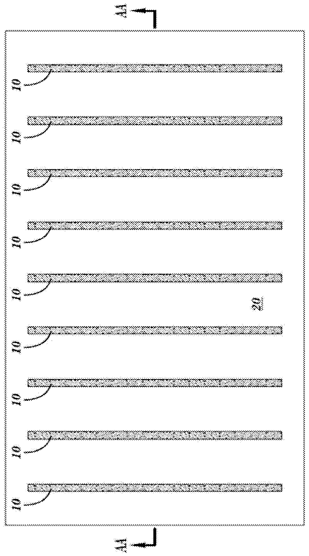
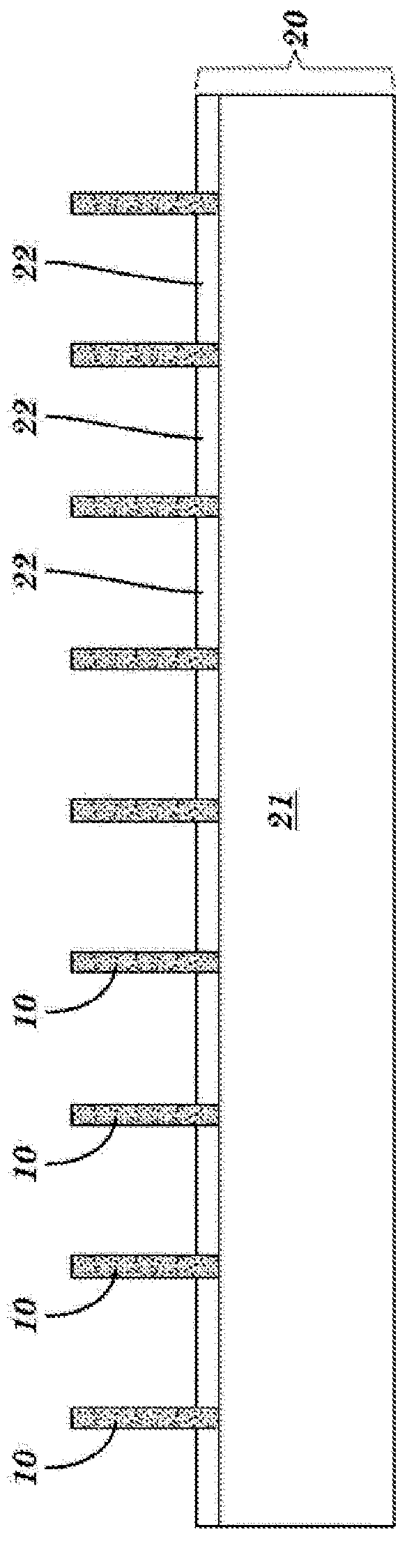
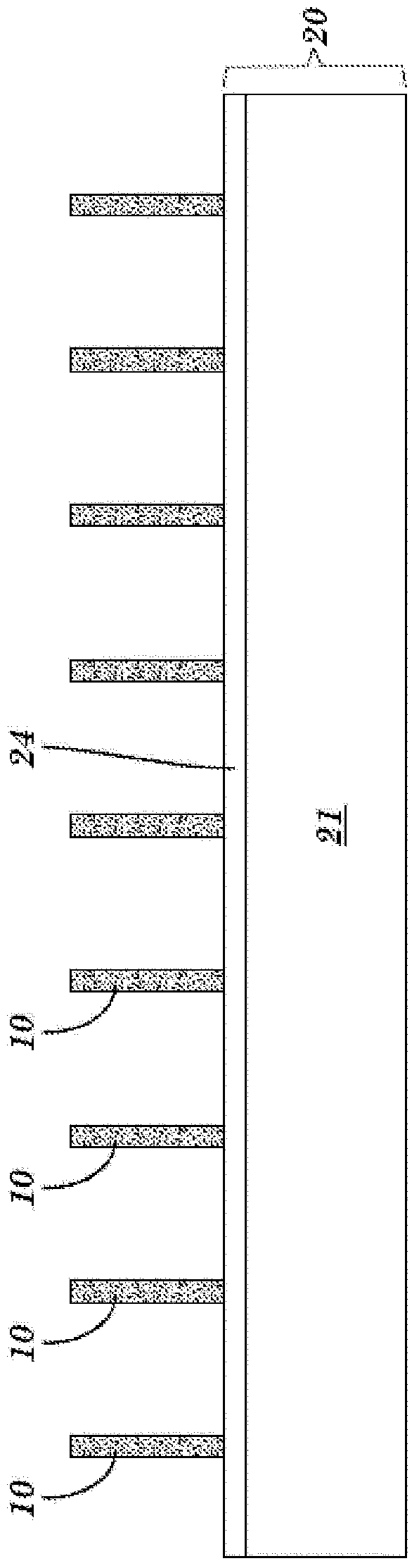
[0022] Figures 1A-1C An array of fins (10) formed on a substrate (20) constituting a preliminary structure for embodiments of the invention is illustrated. Such as Figure 1A As shown in , the fins 10 may have a uniform width and the array of fins may have a uniform pitch. In an embodiment, the width may be in the range of 4nm to 15nm, although small...


PUM


Abstract

Low -resistance contact with the FINFET source / drain can be achieved by forming non -defective surfaces, where this contact is formed on the surface of the non -defective surface.FINFET fins can be exposed to extension growth conditions to increase the volume of semiconductor materials in the source / drain.The front end of the growth can be merged or can be formed.The dielectric material can fill the gap in the source of the polar drain.The grooves separated from the FINFET grid can be exposed to the top of the facial extension of the fins on the fins in the groove. This top is separated by smooth dielectric surface.The selective silicon layer formed on the top exposed in the groove can be converted into a semiconductormetal layer, so that such contact with a separate fin with a separate fins in the source drain area.

Description

technical field [0001] The present disclosure relates to semiconductor structures, and more particularly to FinFET structures and methods of fabrication thereof. Background technique [0002] Fully depleted devices such as Fin Field Effect Transistors (finFETs) are devices used to shrink gate lengths to 14nm and below. Narrow fin structures may be optimal for channel control, but result in increased contact resistance in the source / drain. Larger contact area (and thus less contact resistance) can be provided by incorporating fins in the source / drain, and can be further improved by converting the upper portion of the epitaxial material in the source / drain to silicide Reduce contact resistance. However, epitaxial growth for merging fins has proven challenging. The interface for epitaxial growth from facing fin sidewalls can be defective, and these defects can provide, for example, a better diffusion path for nickel, which can be fatal to the associated device. [0003] A l...

Claims


Application Information

Patent Timeline
Patent Type & Authority Patents(China)
IPC IPC(8): H01L29/78
CPCH01L29/0673H01L29/41791H01L2924/0002H01L29/66795H01L29/785H01L2924/00H01L23/535H01L29/45
Inventor S·纳扎斯V·帕卢楚瑞A·雷茨尼采克D·J·谢皮斯
Owner GLOBALFOUNDRIES INC
Features
  • R&D
  • Intellectual Property
  • Life Sciences
  • Materials
  • Tech Scout
  • Unparalleled Data Quality
  • Higher Quality Content
  • 60% Fewer Hallucinations
Learn More