Method for manufacturing mask plate assembly for evaporation of OLED

A manufacturing method and mask technology, which are applied in vacuum evaporation plating, sputtering plating, ion implantation plating and other directions, can solve the problems of deformation difference, difficult control of precision, uneven physical force, etc., and achieve light weight, The effect of reducing sag and reducing precision offset

Inactive Publication Date: 2016-06-29
KUN SHAN POWER STENCIL
View PDF7 Cites 11 Cited by
  • Summary
  • Abstract
  • Description
  • Claims
  • Application Information

AI Technical Summary

Problems solved by technology

[0006] However, there is still an unavoidable technical problem in the above prior art, because the evaporation region 211 and the non-evaporation region 212 on the mask unit 21 have completely different structures (such as Figure 5 As shown, the vapor deposition area 211 is a through-hole array structure, and the non-evaporation area 212 is a non-through-hole array structure), and the mask unit 21 is stretched by an external mechanism (stretching will cause a certain deformation of the board surface), The physical stress of each area on the surface is not uniform, so the deformation of each area has a certain difference, which makes it difficult to control the position accuracy of the through holes for depositing organic materials on the evaporation area 211 on the mask unit

Method used


Image

  • Method for manufacturing mask plate assembly for evaporation of OLED
  • Method for manufacturing mask plate assembly for evaporation of OLED
  • Method for manufacturing mask plate assembly for evaporation of OLED

Examples


Embodiment Construction

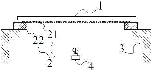
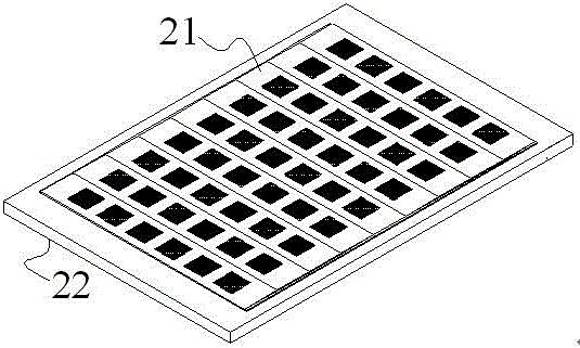
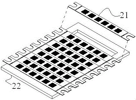
[0057] Embodiments of the present invention are described in detail below, examples of which are shown in the drawings, wherein the same or similar reference numerals designate the same or similar elements or elements having the same or similar functions throughout. The embodiments described below by referring to the figures are exemplary only for explaining the present invention and should not be construed as limiting the present invention.

[0058] In describing the present invention, it should be understood that the terms "upper", "lower", "bottom", "top", "front", "rear", "inner", "outer", "horizontal", " The orientation or positional relationship indicated by "vertical", etc. is based on the orientation or positional relationship shown in the drawings, which is only for the convenience of describing the present invention and simplifying the description, rather than indicating or implying that the device or element referred to must have a specific orientation, so as to Spe...


PUM


Abstract

The invention provides a method for manufacturing a mask plate assembly for evaporation of an OLED. The method comprises the following steps of: S1, a step of manufacturing a mask supporting layer; S2, a step of manufacturing a mask layer; and S3, a step of assembling the mask plate assembly, wherein the mask plate assembly manufactured by virtue of the method comprises at least one mask unit, and each mask unit is composed of two layers of structures including the mask layer and the mask supporting layer. By reasonably arranging the two layers of structures including the mask layer and the mask supporting layer of each mask unit, the mask plate assembly provided by the invention has a relatively high position precision, deposition of an organic material on the surface of a follow-up OLED substrate can be better satisfied, and the quality of an OLED product is effectively improved.

Description

technical field [0001] The invention belongs to the display panel manufacturing industry, and in particular relates to a method for manufacturing a mask plate component for evaporation used in the manufacturing process of an OLED display panel. Background technique [0002] Because organic light-emitting diodes (Organic Light-Emitting Diode, OLED) have self-illumination at the same time, do not need backlight, high contrast, thin thickness, wide viewing angle, fast response speed, can be used for flexible panels, wide temperature range, structure and The excellent characteristics such as relatively simple manufacturing process are considered to be the emerging application technology of the next generation of flat panel displays. [0003] The most important part in the OLED production process is to evaporate the organic layer onto the substrate according to the requirements of the drive matrix to form a key light-emitting display unit. OLED luminescent material is a solid ma...

Claims


Application Information

Patent Timeline
Patent Type & Authority Applications(China)
IPC IPC(8): C23C14/04C23C14/12C23C14/24
CPCC23C14/042C23C14/12C23C14/24
Inventor 魏志凌潘世珎林伟张炜平
Owner KUN SHAN POWER STENCIL
Why Eureka
Try Eureka