Network-on-chip interconnection method and device

An on-chip network and interconnection system technology, applied in the field of on-chip network interconnection methods and devices, can solve problems such as low access efficiency and long frame length, and achieve the effects of being suitable for large-scale popularization and application, easy to implement, and ingenious in design

Active Publication Date: 2016-06-29
炜呈智能电力科技(杭州)有限公司
View PDF2 Cites 9 Cited by
  • Summary
  • Abstract
  • Description
  • Claims
  • Application Information

AI Technical Summary

Problems solved by technology

[0004] In view of this, the purpose of the embodiments of the present invention is to provide a network-on-chip interconnection method and device, so as to improv

Method used


Image

  • Network-on-chip interconnection method and device
  • Network-on-chip interconnection method and device
  • Network-on-chip interconnection method and device

Examples


Embodiment 1

[0053] As we all know, cognitive power line carrier communication is a technology that uses the knowledge of the power line channel environment to improve the efficiency of power line carrier communication. Using this technology, it is possible to detect channel noise and dynamically allocate communication resources according to the detection results. The goal of stabilizing communication probability and improving communication efficiency. Due to the high flexibility of cognitive power line carrier communication, on the one hand, the baseband processor in the communication chip is required to have strong computing power; on the other hand, the baseband processor is also required to support various types of calculations, such as Figure 4 As shown, the embodiment of the present invention provides a schematic diagram of one of the cognitive power line carrier communication chips. P1, ..., P16 in the figure are various types of processors, and R1, ..., R16 are different types of p...

Embodiment 2

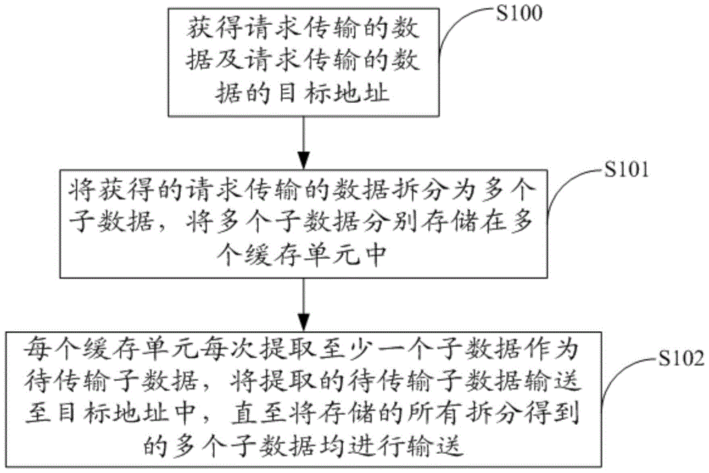
[0084] Such as Figure 8 As shown, the embodiment of the present invention provides an on-chip network interconnection device, including a plurality of cache units 600 for storing data; a splitting unit 601 for obtaining the data requested for transmission and the target address of the data requested for transmission , split the obtained data requested for transmission into a plurality of sub-data, and store the plurality of sub-data in the plurality of cache units 600 respectively; each cache unit 600 in the plurality of cache units 600 uses Each time extracting at least one sub-data from a plurality of stored sub-data as the sub-data to be transmitted, transporting the extracted sub-data to be transmitted to the target address of the data requested for transmission, until all the stored sub-data Multiple sub-data obtained by splitting are all sent.

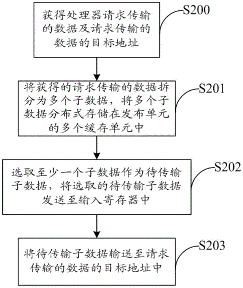
[0085] Based on the above structure, such as Figure 9 As shown, this embodiment provides one of the implementation solution...


PUM


Abstract

The invention provides a network-on-chip interconnection method and a device. A problem in the prior art is solved that that access efficiency is quite low since quite long frame lengths are used in most of network-on-chip interconnection structures. The method comprises steps that a network-on-chip interconnection device obtains data which is requested to be transmitted and a target address of the data which is requested to be transmitted; the obtained data which is requested to be transmitted are divided into multiple sub-data and the sub-data are respectively stored into multiple buffering units; each of the buffering units extracts at least one sub-data from the stored sub-data to be to-be-transmitted sub-data; the extracted to-be-transmitted sub-data is transmitted to the target address of the data which is requested to be transmitted until all the stored sub-data are transmitted. In this way, access frequency can be remarkably increased; and the method and the device satisfy actual demands and are easy to promote and apply.

Description

technical field [0001] The present invention relates to mapping technology, in particular to an on-chip network interconnection method and device. Background technique [0002] Power line carrier communication (powerline carrier communication) is a power system communication in which the transmission line is used as the transmission medium of the carrier signal. Since the transmission line has a very strong support structure and is erected with more than 3 conductors (generally there are three-phase good conductors and one or two overhead ground wires), the transmission line is used to transmit the power frequency current while transmitting the carrier signal. Both economical and reliable. This kind of comprehensive utilization has become the unique means of communication preferred by various electric power departments in the world. In addition, power line carrier communication is a technology that uses the knowledge of the power line channel environment to improve the eff...

Claims


Application Information

Patent Timeline
IPC IPC(8): H04L12/933H04L12/863G06F15/78
CPCG06F15/7825H04L47/6245H04L49/109H04L49/1507
Inventor 陆超
Owner 炜呈智能电力科技(杭州)有限公司
Why Eureka
Try Eureka