Embedded structure of dye-sensitized solar cells and slats for power generation louvers
A technology of solar cells and dye sensitization, applied in photovoltaic power generation, electrical components, electrolytic capacitors, etc., can solve the problems of increased current resistance loss, difficulty in practical application, reduced power generation performance, etc., and achieves reduced resistance and excellent aesthetic properties. , the effect of improving power generation performance
- Summary
- Abstract
- Description
- Claims
- Application Information
AI Technical Summary
Problems solved by technology
Method used
Image
Examples
Embodiment 1
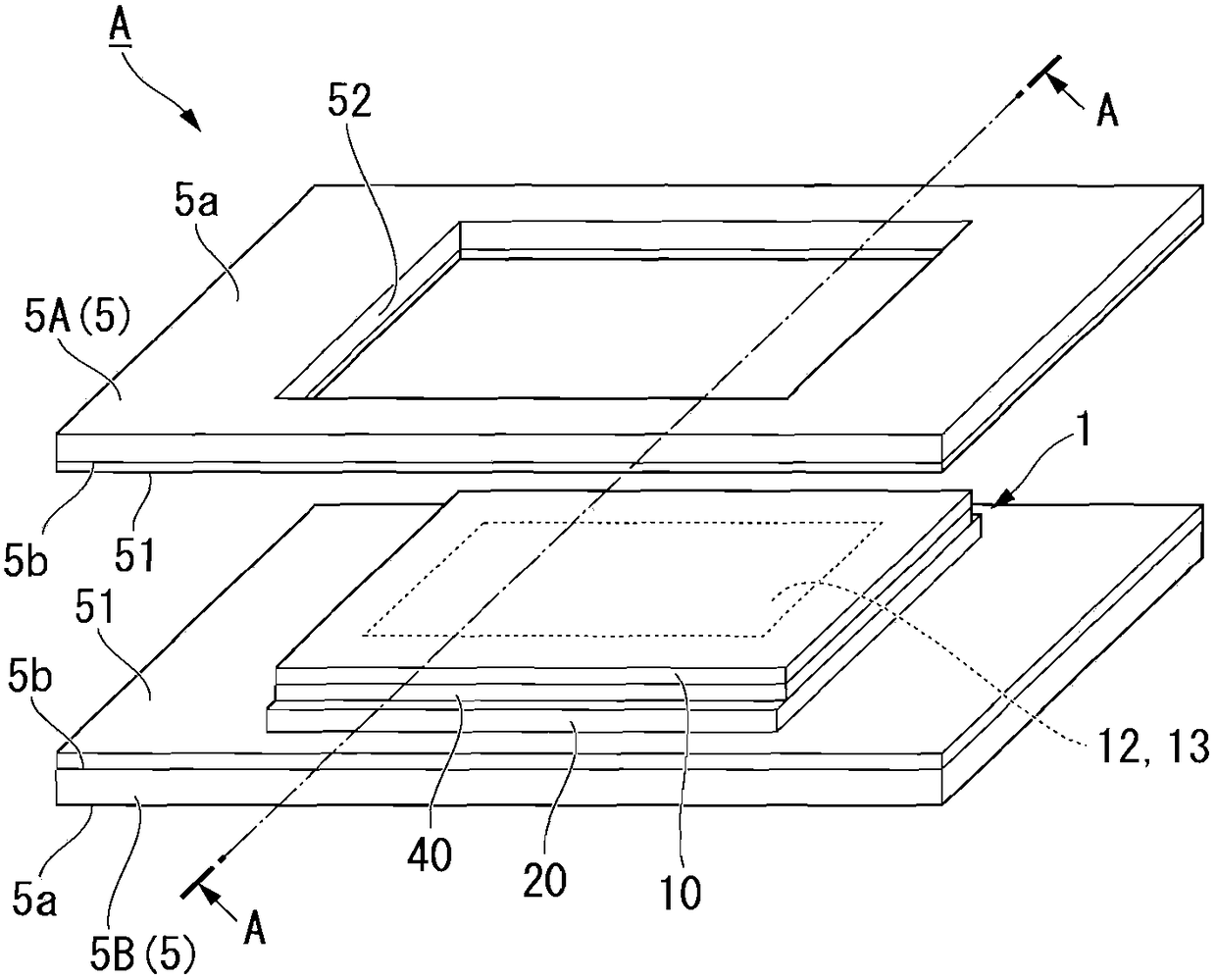
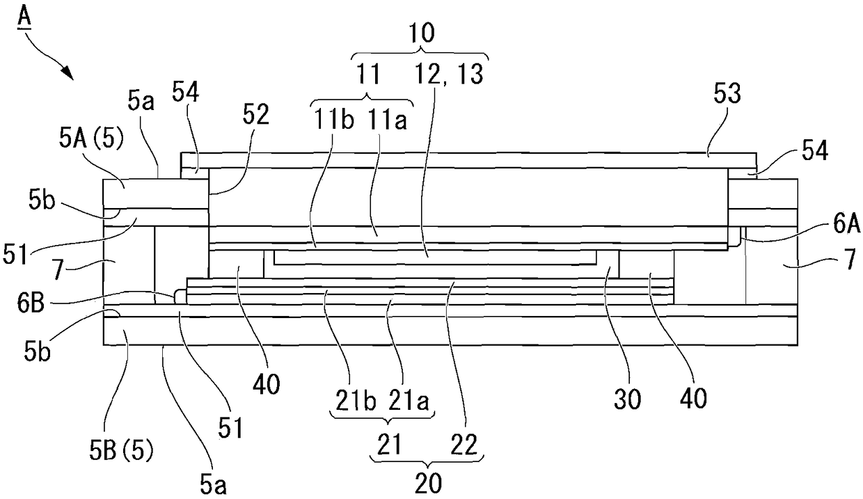
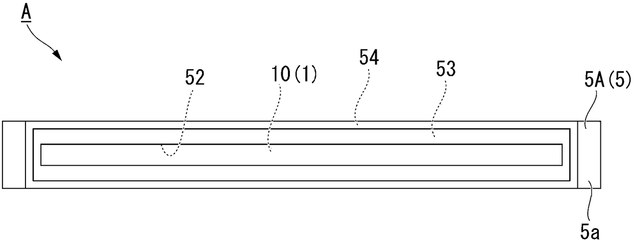
[0152] In Example 1, a photoelectrode and a counter electrode were produced under the following conditions and procedures, a dye-sensitized solar cell was produced between these electrodes, and a pair of conductive layers were formed on one side. The base material is an embedded structure in which a dye-sensitized solar battery cell is inserted between the pair of base materials. In addition, in this example, as an example of the embedding structure of the dye-sensitized solar cell to which the present invention is applicable, a louver in which the dye-sensitized solar cell is embedded was produced.
[0153] (Production of photoelectrode)
[0154] First, as a conductive resin substrate, prepare a 15mm×214mm ITO (indium tin oxide)-PEN (polyethylene naphthalate) film material (sheet resistance: 15Ω / □), and use AD Titanium oxide particles described below were blown by the method to form a semiconductor layer. At this time, as film-forming conditions of the AD method, nitrogen w...
Embodiment 2
[0184] In Example 2, the dye-sensitized solar cell of the present invention was produced in the same procedure as in Example 1, except that aluminum was vapor-deposited as a conductive layer on one side of the pair of base materials of the slats to be a louver. An example of the embedded structure, that is, blinds, were evaluated in the same way. At this time, the film thickness of the conductive layer was adjusted so that the sheet resistance of the conductive layer was 3Ω / □.
PUM
 Abstract
Description
Claims
Application Information


