High-resistance ZnO thin film based photoconductive X-ray detector and preparation method therefor

A photoconductive and X-ray technology, applied in the direction of semiconductor devices, circuits, electrical components, etc., to achieve the effects of reducing noise, reducing production costs, improving sensitivity and fast response characteristics

Inactive Publication Date: 2016-07-06
XI AN JIAOTONG UNIV
View PDF5 Cites 14 Cited by
  • Summary
  • Abstract
  • Description
  • Claims
  • Application Information

AI Technical Summary

Problems solved by technology

Especially compared with other wide bandgap semiconductors such as diamond, SiC, GaN, etc., the low-cost preparation method of ZnO single crystal and thin film crystal has incomparable advantages, but there is no detector in the prior art that has low noise, High sensitivity, fast response and low cost characteristics

Method used


Image

  • High-resistance ZnO thin film based photoconductive X-ray detector and preparation method therefor
  • High-resistance ZnO thin film based photoconductive X-ray detector and preparation method therefor
  • High-resistance ZnO thin film based photoconductive X-ray detector and preparation method therefor

Examples


Embodiment Construction

[0027] The present invention is described in further detail below in conjunction with accompanying drawing:

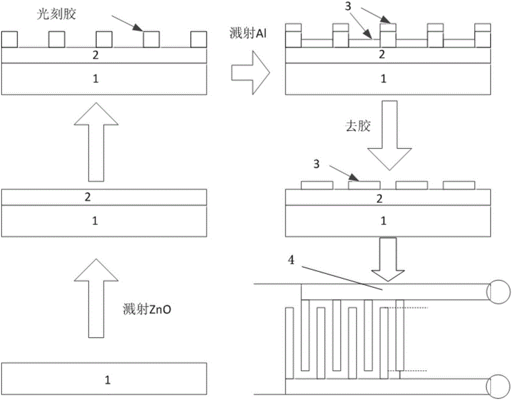
[0028] refer to figure 1 The photoconductive X-ray detector based on the high-resistance ZnO thin film of the present invention includes a housing, two lead wires 4, and an electrode layer, a ZnO film layer 2 and a lining that are arranged in the housing and arranged in sequence from top to bottom. The bottom substrate 1, the electrode layer is composed of several Al films 3 distributed at equal intervals, one lead 4 is connected to a part of the Al film 3, the other lead 4 is connected to another part of the Al film 3, and connected to two leads 4. 4 connected Al film 3 staggered distribution.

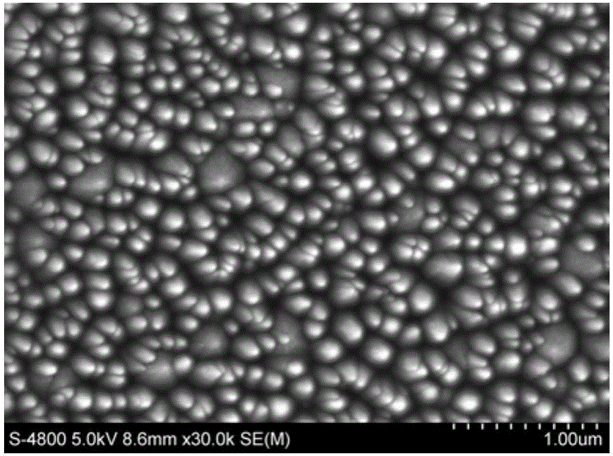
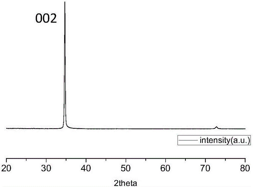
[0029] It should be noted that the thickness of the ZnO film layer 2 is greater than or equal to 1 μm, and the resistivity of the ZnO film layer 2 is greater than or equal to 1×10 8 Ω·cm; Substrate 1 is glass substrate, quartz substrate or with SiO 2 Si substrate; the dista...


PUM


Abstract

The invention discloses a high-resistance ZnO thin film based photoconductive X-ray detector and a preparation method therefor. The photoconductive X-ray detector comprises a shell, two leads, and an electrode layer, a ZnO film layer and a substrate which are arranged in the shell from upper to lower in sequence; the electrode layer comprises multiple Al films distributed at equal intervals; one lead is connected with a part of the Al films while the other lead is connected with the other part of the AL films; and the AL films connected with two leads are distributed in a staggered manner. The photoconductive X-ray detector has the characteristics of low noise, high sensitivity and rapid response, as well as relatively low preparation cost.

Description

technical field [0001] The invention belongs to the field of semiconductor nuclear radiation X-ray detection devices, and relates to a photoconductive X-ray detector based on a high-resistance ZnO thin film and a preparation method thereof. Background technique [0002] With the continuous development of X-ray detection in nuclear energy, nuclear safety, medical imaging and aerospace applications, there is an urgent need for high-sensitivity, low-noise and low-cost detector technology. Si and Ge devices based on narrow-bandgap semiconductors and detectors such as CdTe and CdZnTe with medium bandgap have been put into practical use, but they still face challenges in wide temperature range operation, radiation resistance and low cost. Institutions such as Oak Ridge National Laboratory in the United States, Lawrence Livermore National Laboratory, Pacific Northwest National Laboratory and the University of Saskatchewan in Canada are actively developing various new wide-bandgap s...

Claims


Application Information

Patent Timeline
Patent Type & Authority Applications(China)
IPC IPC(8): H01L31/08H01L31/0296H01L31/0224H01L31/18
CPCH01L31/0224H01L31/0296H01L31/085H01L31/1828H01L31/1836Y02P70/50
Inventor 贺永宁黄志永赵小龙祁晓萌彭文博陈亮欧阳晓平
Owner XI AN JIAOTONG UNIV
Why Eureka
Try Eureka