Manufacturing method of PCB, and PCB

A manufacturing method and a technology for protecting cover plates, which are applied in the fields of printed circuit manufacturing, components of lighting devices, lighting and heating equipment, etc., can solve complex processes, large equipment space, and inability to achieve higher density and high integration LED packaging, etc. problems, to achieve the effect of improving alignment accuracy, improving pass rate and reliability

Active Publication Date: 2016-07-13
DONGGUAN SHENGYI ELECTRONICS
View PDF4 Cites 2 Cited by
  • Summary
  • Abstract
  • Description
  • Claims
  • Application Information

AI Technical Summary

Problems solved by technology

At present, LAMP packaging and SMD packaging technologies are commonly used in the LED packaging industry to assemble LEDs and PCBs, but limited by the overall size and pin size of a single LED, it is impossible to achieve higher density and more integrated LED packaging. LED packages with center-to-cent...

Method used


Image

  • Manufacturing method of PCB, and PCB
  • Manufacturing method of PCB, and PCB
  • Manufacturing method of PCB, and PCB

Examples


Embodiment 1

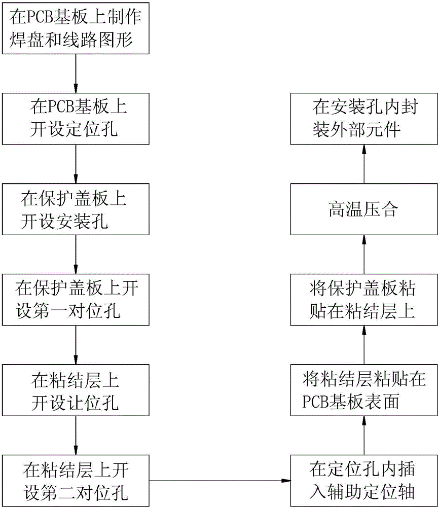
[0088] Such as Figures 1 to 8 As shown, on the one hand, a method for manufacturing a PCB is provided, comprising the following steps:

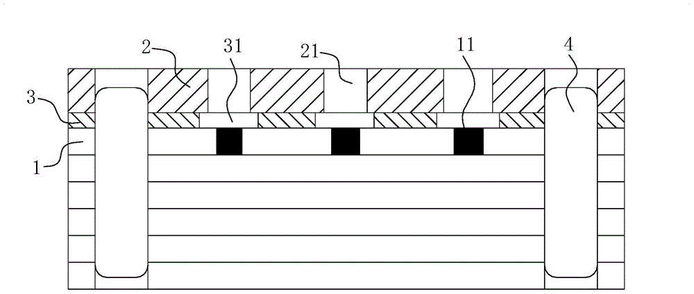
[0089] S10 , providing a PCB substrate 1 , and making pads 11 and circuit patterns on the surface of the PCB substrate 1 . In this embodiment, the PCB substrate 1 is a multilayer PCB substrate made of high-strength substrate materials.

[0090] S20 , making a solder resist layer on the surface of the PCB substrate 1 , the solder resist layer is a black solder resist layer.

[0091] S30 , fabricating an electroless nickel gold layer or an electroplated gold layer on the surface of the PCB substrate 1 .

[0092] S40 , opening a positioning hole 12 on the PCB substrate 1 .

[0093] S50 , performing wet electroplating on the positioning hole 12 to improve the wear resistance of the positioning hole 12 .

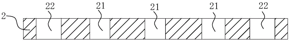
[0094] S60 , providing a protective cover 2 , and opening mounting holes 21 on the protective cover 2 for the pads 11 on the surface of th...

Embodiment 2

[0113] Such as Figures 1 to 5 shown, and as Figures 9 to 11 As shown, on the one hand, a method for manufacturing a PCB is provided, comprising the following steps:

[0114] S10 , providing a PCB substrate 1 , and making pads 11 and circuit patterns on the surface of the PCB substrate 1 . In this embodiment, the PCB substrate 1 is a single-sided PCB substrate 1 made of high-strength substrate material.

[0115] S20 , making a solder resist layer on the surface of the PCB substrate 1 , the solder resist layer is a white solder resist layer.

[0116] S30 , fabricating an electroless nickel gold layer or an electroplated gold layer on the surface of the PCB substrate 1 .

[0117] S40 , opening a positioning hole 12 on the PCB substrate 1 .

[0118] S50 , performing wet electroplating on the positioning hole 12 to improve the wear resistance of the positioning hole 12 .

[0119] S60 , providing a protective cover 2 , and opening mounting holes 21 on the protective cover 2 f...

Embodiment 3

[0138] Such as Figures 1 to 5 shown, and as Figures 9 to 11As shown, on the one hand, a method for manufacturing a PCB is provided, comprising the following steps:

[0139] S10 , providing a PCB substrate 1 , and making pads 11 and circuit patterns on the surface of the PCB substrate 1 . In this embodiment, the PCB substrate 1 is a double-sided PCB substrate 1 made of high-strength substrate material.

[0140] S20 , making a solder resist layer on the surface of the PCB substrate 1 , the solder resist layer is a white solder resist layer.

[0141] S30 , fabricating an electroless nickel gold layer or an electroplated gold layer on the surface of the PCB substrate 1 .

[0142] S40 , opening a positioning hole 12 on the PCB substrate 1 .

[0143] S50 , performing wet electroplating on the positioning hole 12 to improve the wear resistance of the positioning hole 12 .

[0144] S60 , providing a protective cover 2 , and opening mounting holes 21 on the protective cover 2 fo...


PUM

PropertyMeasurementUnit
Thicknessaaaaaaaaaa
Diameteraaaaaaaaaa
Thicknessaaaaaaaaaa

Abstract

The invention discloses a manufacturing method of a PCB, and a PCB manufactured by use of the method. The PCB comprises a PCB substrate and a protective cover plate. The protective cover plate is adhered to the PCB substrate through an adhesive coating, the adhesive coating is prepared by a low-flow glue material or a flow-free glue material, the PCB substrate is provided with a pad and a positioning hole, an installation hole is arranged at a position, corresponding to the pad, of the protective cover plate, a relief hole is arranged at a position, corresponding to the pad, of the adhesive coating, an LED chip is packaged inside the installation hole, the LED chip is electrically connected with the PCB substrate through the pad, alignment holes are arranged at positions, corresponding to the positioning hole, of the protective cover plate and the adhesive coating, and the positioning hole and the alignment holes are selectively aligned through an auxiliary positioning shaft. According to the invention, through a cooperative structure of the PCB substrate, the adhesive coating and the protective cover plate, gummosis on the surface of the pad position of the PCB substrate is avoided, and the integration density of the LED chip is improved. Besides, through a cooperative structure of the positioning hole, the alignment holes and the auxiliary positioning shaft, the alignment precision of the protective cover plate and the PCB substrate is effectively improved.

Description

technical field [0001] The invention relates to the technical field of PCB processing, in particular to a PCB manufacturing method and the PCB. Background technique [0002] In people's life and work, electronic products play an increasingly important role, people rely more and more on electronic products, and at the same time, people have higher and higher requirements for the portability of electronic products. This demand makes electronic products continuously improve toward the direction of high integration and miniaturization, among which, the demand for high integration and miniaturization of PCB is particularly obvious. [0003] The surface of the PCB is generally provided with many components, and LED is one of the more common ones. Therefore, the package or mounting structure of LED and PCB is an important factor affecting the high integration and miniaturization of PCB. At present, LAMP packaging and SMD packaging technologies are commonly used in the LED packagin...

Claims


Application Information

Patent Timeline
IPC IPC(8): H05K3/30H05K3/34F21V19/00
CPCF21V19/003H05K3/303H05K3/341H05K2203/304
Inventor 李民善纪成光袁继旺陈正清胡源梁尉坚
Owner DONGGUAN SHENGYI ELECTRONICS
Why Eureka
Try Eureka