Optoelectronic components and methods for their manufacture

A component, optoelectronic technology, applied in electrical components, electro-solid devices, circuits, etc., can solve problems such as process speed reduction, achieve rapid and safe identification, and save method steps.

Active Publication Date: 2018-06-19
OSRAM OPTO SEMICON GMBH & CO OHG
View PDF6 Cites 0 Cited by
  • Summary
  • Abstract
  • Description
  • Claims
  • Application Information

AI Technical Summary

Problems solved by technology

The orientation marks have to be approached several times during the assembly process, which results in a significant reduction in process speed

Method used


Image

  • Optoelectronic components and methods for their manufacture
  • Optoelectronic components and methods for their manufacture
  • Optoelectronic components and methods for their manufacture

Examples


Embodiment Construction

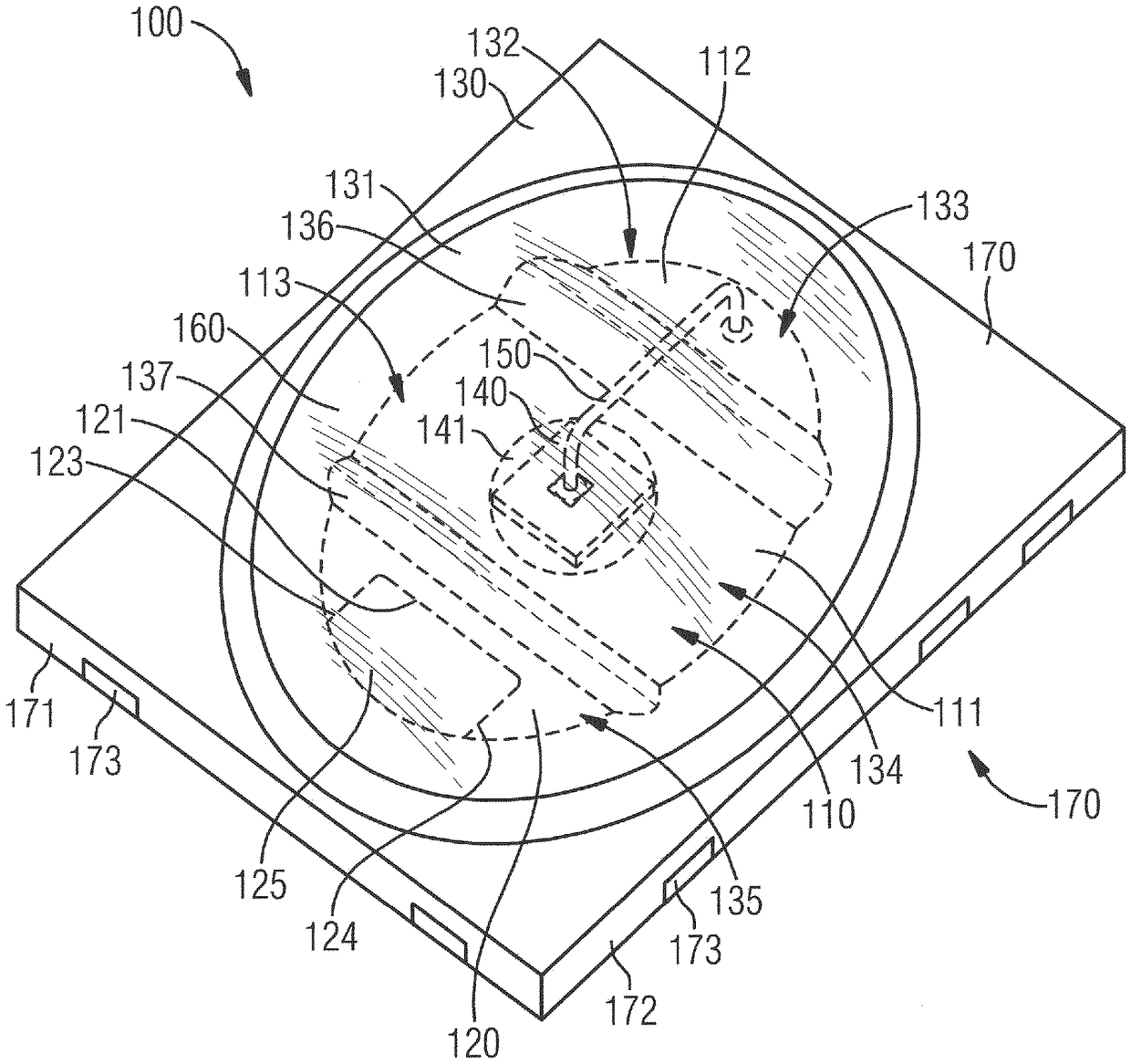
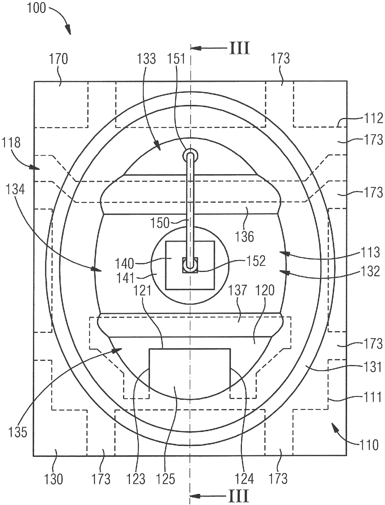
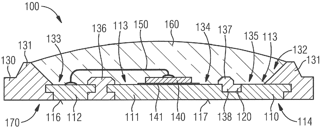
[0041] figure 1 Shows a perspective view of an optoelectronic component 100 designed according to a first embodiment of the invention, comprising a carrier 170 , an optoelectronic semiconductor chip 140 mounted on the carrier and an Housing 131. Here, used as a carrier is a lead frame 110 embedded in a molded body 130 formed of molding material. The housing 131 is designed in the present example with an elliptical contour which forms the cavity 132 for receiving the optoelectronic semiconductor chip 140 . The cavity 132 is divided into three sections 133 , 134 , 135 by two web-shaped structures extending transversely to the longitudinal axis of the elliptical housing. The optoelectronic semiconductor chip 140 is mounted directly on the surface of the frame element 110 in the central section 134 of the cavity 132 by means of solder or adhesive particles 141 . The lead frame 110 is constructed in two parts, wherein the semiconductor chip is fastened on the first lead frame pa...


PUM


Abstract

The invention relates to a method for producing an optoelectronic component (100) comprising a lead frame (110) embedded in a molded body (130) and arranged on the upper side (113) of the lead frame (110) Optoelectronic semiconductor chip (140) on. Here a lead frame (110) is provided. In a further step, an etching step is performed in which at least one trench structure ( 120 ) is produced in the lead frame ( 110 ) on the upper side ( 113 ) of the lead frame ( 110 ). Furthermore, the molded body ( 130 ) is produced by overmolding the lead frame ( 110 ) with a molding material by injection molding. In addition, an optoelectronic semiconductor chip (140) is arranged on the upper side (113) of the lead frame (110), wherein at least one trench structure (120) is used for arranging the optoelectronic semiconductor chip (140) on the lead frame (110) Orientation mark for up orientation.

Description

technical field [0001] The invention relates to a photovoltaic component and a method for producing a photovoltaic component. Background technique [0002] This patent application claims priority from German patent application 10 2013 224 581.5, the disclosure content of which is hereby accepted by reference. [0003] An optoelectronic component generally comprises one or more optoelectronic semiconductor chips for generating optical radiation and a carrier serving as a housing for the semiconductor chips. The optoelectronic semiconductor chip is, for example, a light emitting diode chip (LED, Light Emitting Diode), wherein, depending on the application, conversion elements for radiation conversion can be arranged on the light emitting diode chip. Usually used as a carrier here is a lead frame in which a metal is embedded in a molded body made of a molding material. In this case, the molded body is usually produced by overmolding the lead frame with plastic, epoxy resin or...

Claims


Application Information

Patent Timeline
Patent Type & Authority Patents(China)
IPC IPC(8): H01L33/48H01L33/62H01L33/00
CPCH01L33/486H01L2933/0033H01L2933/0066H01L2224/32245H01L2224/48247H01L2224/73265H01L2224/92247H01L2924/181H01L2224/48464H01L2924/00014G10L2015/223H01L33/62H01L2924/00H01L2224/05599H01L2224/45099H01L2224/85399H01L2924/00012H01L24/48H01L33/54H01L2933/005
Inventor 安德列亚斯·格林迪托比亚斯·格布赫尔马库斯·平德尔
Owner OSRAM OPTO SEMICON GMBH & CO OHG
Why Eureka
Try Eureka