
A kind of semiconductor laser based on anisotropic substrate
An anisotropic, laser technology, applied in semiconductor lasers, the structural details of semiconductor lasers, lasers, etc., can solve the problems of low heat conduction efficiency and complex packaging process, to simplify manufacturing process steps, improve heat dissipation efficiency, and reduce precision. Effect
Patent Information
- Authority / Receiving Office
- CN · China
- Patent Type
- Patents(China)
- Current Assignee / Owner
- Publication Date
- 2019-02-26
Smart Images
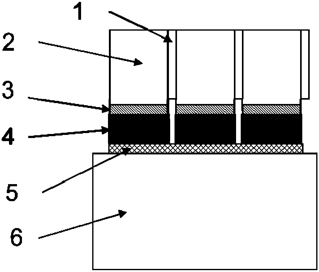
Figure 1 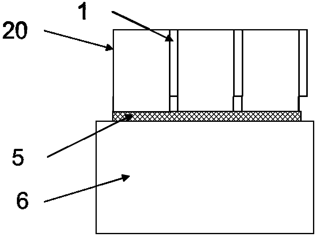
Figure 2 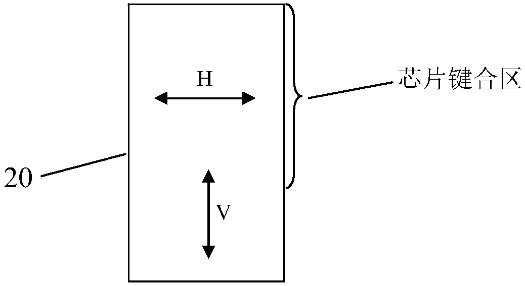
Figure 3
Abstract
Description
technical field
[0001] The invention relates to a semiconductor laser, and mainly relates to the improvement of the chip substrate. Background technique
[0002] like figure 1 A common semiconductor laser packaging structure is shown, the heat dissipation path of the laser chip is as follows: the heat generated by the semiconductor laser chip 1 is first conducted to the substrate 2, then to the insulating block 4 through the solder layer 3, and then through the solder layer 5 is conducted to the radiator 6. The heat conduction path from the laser chip to the heat sink is long and there are many interfaces, which reduces the heat dissipation capability of the entire laser.
[0003] Due to the requirements of structure and process, the thickness of the insulating block 4 generally needs to reach more than 300 microns, which also limits its heat conduction efficiency. At the same time, the solder layer is required for assembly and bonding between the insulating block, the la...
Examples
Embodiment Construction
[0037] like figure 2 As shown, the laser chip 1 is assembled on a substrate 20 with high thermal conductivity and CTE matching, and one or more laser chips and the corresponding substrate are assembled and bonded to the radiator 6 through solder 5 to form a semiconductor laser. The substrate has conductivity in the chip stacking direction (the conductive area covers at least the chip bonding area), and has insulation in the direction perpendicular to the surface of the heat sink.
[0038] like image 3 , the substrate 20 is a composite body composed of insulating materials and conductive materials. The insulating material and the conductive material are closely combined. Such an integrated substrate realizes both conduction and insulation. Compared with the existing conductive substrate plus insulating block bonding The combination of two bonded interfaces and a solder layer (5 to 10 microns thick) are reduced. The layout of the insulating material and the conductive materi...