Supercharge Your Innovation With Domain-Expert AI Agents!

Display panel as well as production method and display device thereof

A technology for a display panel and a manufacturing method, applied in the fields of display panels and display devices, capable of solving problems such as carcinogenicity and environmental pollution

Active Publication Date: 2016-07-27
BOE TECH GRP CO LTD +1
View PDF4 Cites 13 Cited by
  • Summary
  • Abstract
  • Description
  • Claims
  • Application Information

AI Technical Summary

Problems solved by technology

[0003] Embodiments of the present invention provide a display panel, its manufacturing method and display device, which are used to solve the problems of environmental pollution and carcinogenesis caused by the use of toxic chromium ions in the black matrix in the prior art

Method used


Image

  • Display panel as well as production method and display device thereof
  • Display panel as well as production method and display device thereof
  • Display panel as well as production method and display device thereof

Examples


Embodiment Construction

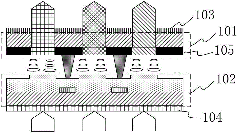
[0028] Aiming at the problems existing in the prior art, such as environmental pollution and carcinogenicity caused by the use of toxic chromium ions in the black matrix, the embodiments of the present invention provide a display panel, a manufacturing method thereof, and a display device.

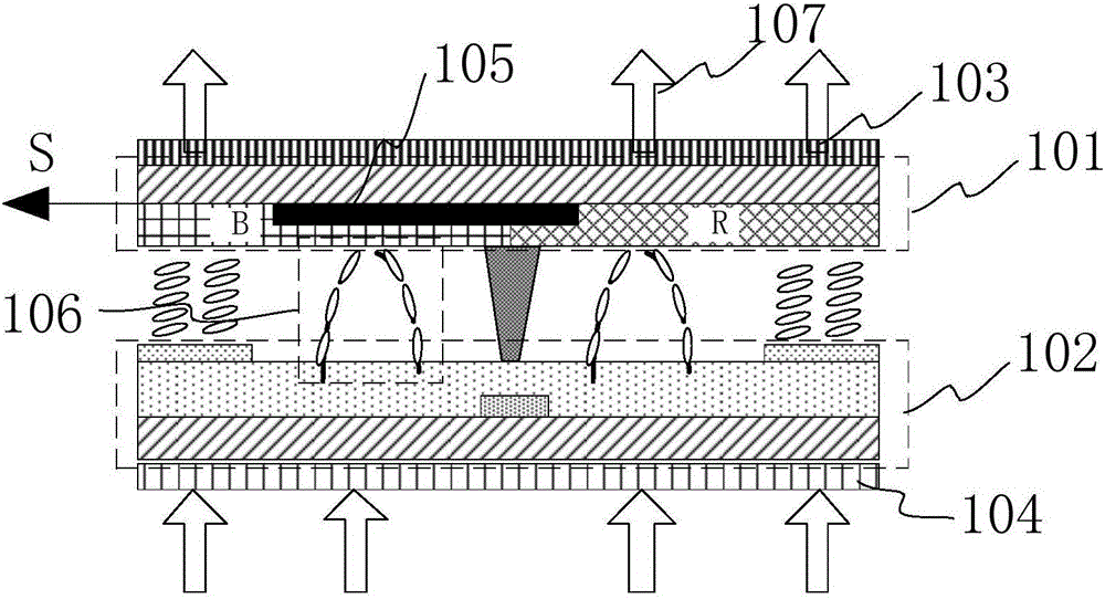
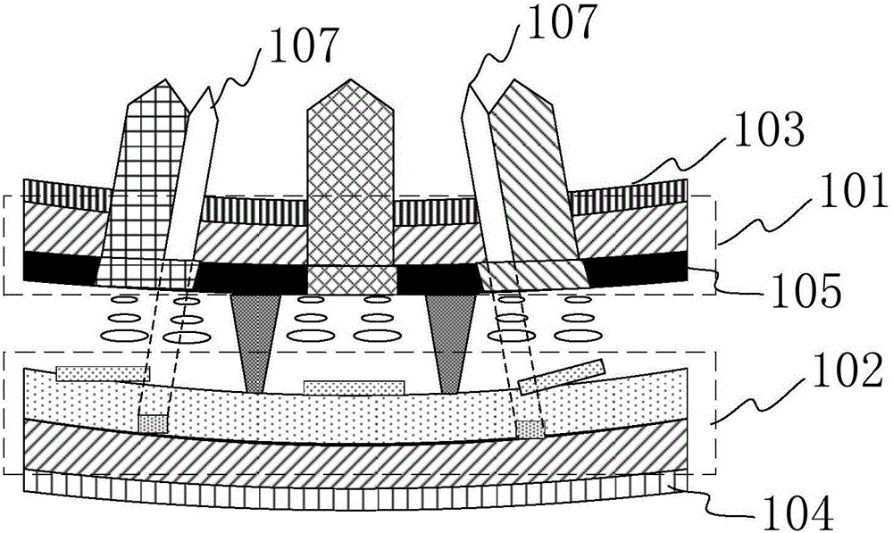
[0029] First, refer to Figure 4 , the present invention provides a display panel, comprising: a first substrate 201 and a second substrate 202 facing each other, a liquid crystal layer 203 located between the first substrate 201 and the second substrate 202, a liquid crystal layer 203 located on the first substrate 201 away from the liquid crystal The first polarizer 204 on one side of the layer 203, and the second polarizer 205 located on the side of the second substrate 202 away from the liquid crystal layer 203; the light absorption axis directions of the first polarizer 204 and the second polarizer 205 are perpendicular to each other ,Also includes:

[0030] The polarizing film layer...


PUM


Abstract

The invention discloses a display panel as well as a production method and a display device thereof. The display panel comprises a first substrate and a second substrate, a liquid crystal layer, a first light deflecting sheet and a second light deflecting sheet, wherein the first substrate is arranged to be opposite to the second substrate, the liquid crystal layer is located between the first substrate and the second substrate, the first light deflecting sheet is located at one side, deviated from the liquid crystal layer of the first substrate, the second light deflecting sheet is located at one side, deviated from the liquid crystal layer, of the second substrate, and light absorption axes of the first light deflecting sheet and the second light deflecting sheet are vertical to each other in direction. The display panel further comprises a membrane layer, wherein membrane layer having light deflecting characteristics is arranged at one side, deviated from the first light deflecting sheet, of the first substrate as a black matrix, and the membrane layer having the light deflecting characteristics is vertical to a light absorption axis of the first light deflecting sheet in direction. As the membrane layer having the light deflecting characteristics is arranged to be vertical to the light absorption axis of the first light deflecting sheet in direction, light rays cannot penetrate through patterned positions of the membrane layer having the light deflecting characteristics, so that the black matrix is replaced, and the use of chromium ions which are carcinogenic and are not environmentally-friendly is avoided.

Description

technical field [0001] The invention relates to the technical field of liquid crystal display, in particular to a display panel, a manufacturing method thereof and a display device. Background technique [0002] like figure 1 As shown, a thin film transistor display panel (thinfilm transistor-liquid crystal display, TFT-LCD) generally includes a color filter (ColorFilter, CF) substrate 101 and an array (Array) substrate 102, filling the liquid crystal (Liquid crystal, LC) layer between them, and Polarizer layers perpendicular to the substrate surfaces on both sides of the upper and lower sides ( figure 1 103 and 104 in ). After an external voltage signal is applied to the array substrate 102, the deflection of the liquid crystal molecules in the display area is controlled; through the birefringence of the liquid crystal molecules, the adjustment of the transmitted light is realized. The circularly polarized light of the backlight passes through the polarizer on the array ...

Claims


Application Information

Patent Timeline
Patent Type & Authority Applications(China)
IPC IPC(8): G02F1/1335
CPCG02F1/133512G02F1/133528G02F1/133531G02B1/08G02F1/136209G02F2203/68G03F7/0007G03F7/105G02F1/133538G02F1/133565C09K2323/031G02F1/133514G03F7/0045G03F7/16G03F7/20
Inventor 江亮亮
Owner BOE TECH GRP CO LTD
Features
  • R&D
  • Intellectual Property
  • Life Sciences
  • Materials
  • Tech Scout
  • Unparalleled Data Quality
  • Higher Quality Content
  • 60% Fewer Hallucinations
Learn More