
A high-power and large-bandwidth germanium-silicon photodetector

A photodetector and large bandwidth technology, which is applied in the direction of circuits, electrical components, semiconductor devices, etc., can solve the problems of incompatibility of comprehensive performance such as output power, operating bandwidth and device design complexity, and achieve compact structure and saturated output power The effect of height and area increase

Active Publication Date: 2018-05-22
HUAZHONG UNIV OF SCI & TECH
View PDF2 Cites 0 Cited by
  • Summary
  • Abstract
  • Description
  • Claims
  • Application Information

AI Technical Summary

Problems solved by technology

[0005] The technical problem to be solved by the present invention is to provide a high-power and large-bandwidth germanium-silicon photodetector to overcome the problem that the comprehensive performance of the existing germanium-silicon photodetector is difficult to be compatible, such as output power, working bandwidth and device design complexity.

Method used


Image

  • A high-power and large-bandwidth germanium-silicon photodetector
  • A high-power and large-bandwidth germanium-silicon photodetector
  • A high-power and large-bandwidth germanium-silicon photodetector

Examples


Embodiment Construction

[0029] In order to make the object, technical solution and advantages of the present invention clearer, the present invention will be further described in detail below in conjunction with the accompanying drawings and embodiments. It should be understood that the specific embodiments described here are only used to explain the present invention, not to limit the present invention. In addition, the technical features involved in the various embodiments of the present invention described below can be combined with each other as long as they do not constitute a conflict with each other.

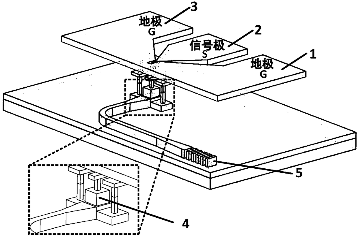
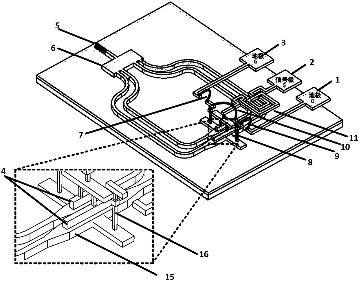
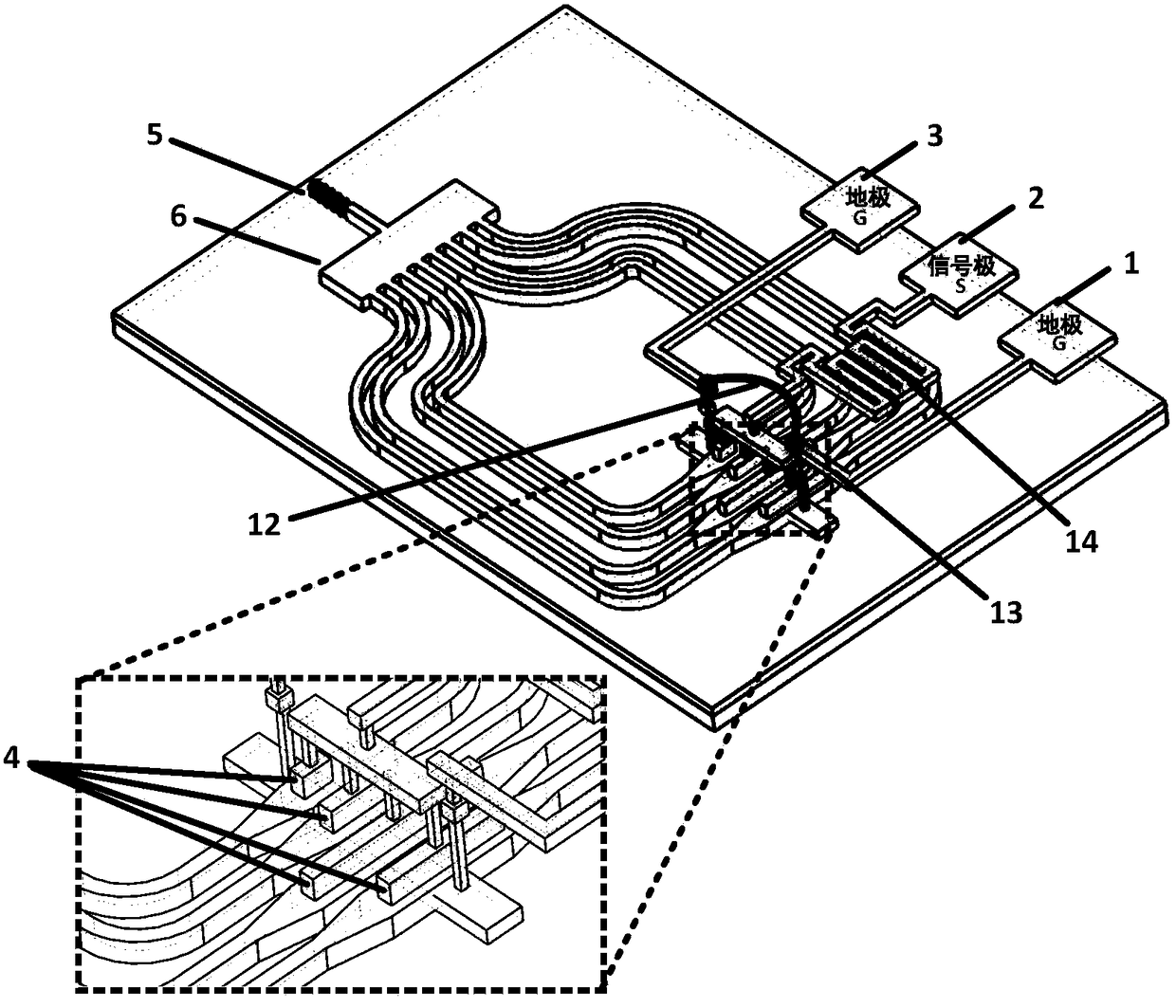
[0030] compared to figure 1 Existing SiGe detectors such as figure 2 Shown is a structural schematic diagram of a specific implementation of the high-power and wide-bandwidth silicon-germanium photodetector of the present invention (Example 1). The working principle, implementation conditions and steps of the present invention will be described in detail below in conjunction with related devi...


PUM


Abstract

The invention discloses a high-power broadband germanium-silicon photoelectric detector. The detector is used for simulating silicon-based key integrated photoelectric devices of a photon communication system and a microwave photon system, wherein the detector is characterized by comprising multiple shunt-wound germanium-layer structures and inductors. The multiple germanium layers of the shunt-wound germanium-layer structures can be different in sizes to realize regulation and control on parasitic resistance so as to improve the saturation power of the device and ensure that that parasitic parameters are not obviously increased as well; meanwhile, an on-chip inductor and an off-chip inductor are introduced, so that the regulation and control for the parasitic resistance of the device is realized, the high-frequency response of the device is improved, and the operating bandwidth of the device is enhanced; and in addition, the photoelectric detector provided by the invention adopts a lumped electrode structure, so that the germanium-silicon photoelectric detector with high power, broad band, and compact structure is realized.

Description

technical field [0001] The invention relates to a silicon-based integrated optoelectronic device in an analog photonic communication system or a microwave photonic system, and more particularly relates to a silicon-germanium photodetector with high power and wide bandwidth for converting optical signals into electrical signals. Background technique [0002] In the fields of analog photonic communication, microwave photonics, etc., detectors with high saturation power and large bandwidth are required to convert optical signals into electrical signals. The existing detectors based on group III-V materials are technically characterized by high saturation power and wide bandwidth, but there are problems such as high cost and unfavorable large-scale integration. [0003] Xianshu Luo et al. disclose a silicon germanium photodetector using a multi-level cascaded germanium layer structure and a traveling wave electrode structure to increase the saturation power of an output electric...

Claims


Application Information

Patent Timeline
Patent Type & Authority Patents(China)
IPC IPC(8): H01L31/105H01L31/02
CPCH01L31/02019H01L31/105
Inventor 余宇陈冠宇张新亮
Owner HUAZHONG UNIV OF SCI & TECH
Learn More