OLED display panel and manufacturing method

A technology for display panels and manufacturing methods, applied to instruments, electrical digital data processing, and input/output processes of data processing, etc., can solve problems such as unfavorable small electronic device design, increased frame size, easy misalignment, etc., and achieve shortened communication Effects of distance, reduced module thickness, and reduced number of components

Active Publication Date: 2016-08-03
SUZHOU QUINGYUE OPTOELECTRONICS TECH CO LTD
View PDF5 Cites 11 Cited by
  • Summary
  • Abstract
  • Description
  • Claims
  • Application Information

AI Technical Summary

Problems solved by technology

However, in order to ensure the wiring space of the NFC antenna in such a solution, the NFC wire frame must be made very large, thereby increasing the frame size of the entire module outside the display area
This solution solves the problem of easy wear and misalignment of conventional NFC antenna wiring to a certain extent, but the excessively large module frame size is also not conducive to the design of small electronic devices

Method used


Image

  • OLED display panel and manufacturing method
  • OLED display panel and manufacturing method
  • OLED display panel and manufacturing method

Examples


Embodiment Construction

[0039] In order to further explain the technical means and effects of the present invention to achieve the intended purpose of the invention, the specific implementation, structure, features and effects of the present invention will be described in detail below in conjunction with the accompanying drawings and examples.

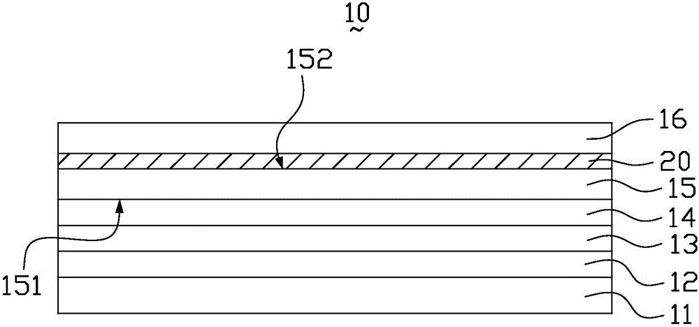
[0040] figure 1 For the schematic structural diagram of the OLED display panel in the first embodiment of the present invention, please refer to figure 1The OLED display panel 10 includes an OLED screen encapsulation cover 11 , an OLED first electrode 12 , an OLED light emitting region 13 , an OLED second electrode 14 , an OLED substrate 15 and an insulating protective film 16 which are stacked in sequence. Specifically, the OLED first electrode 12 is arranged on the OLED screen body packaging cover 11, the OLED light-emitting area 13 is arranged on the OLED first electrode 12, the OLED second electrode 14 is arranged on the OLED light-emitting area 13, and t...


PUM


Abstract

The invention discloses an OLED (Organic Light-Emitting Diode) display panel and a manufacturing method. The OLED display panel comprises an OLED screen body packaging cover, a first OLED electrode, an OLED luminous area, a second OLED electrode, an OLED substrate and an insulating protective film, which are sequentially cascaded, wherein the OLED substrate is provided with a first surface facing the OLED luminous area and a second surface facing one side of the insulating protective film; the second OLED electrode is positioned on one side of the first surface of the OLED substrate; an NFC (Near Field Communication) antenna wire is formed on the second surface of the OLED substrate, and is covered by the insulating protective film; light for display is emitted to the side where the OLED substrate is positioned by the OLED luminous area to make the NFC antenna wire be positioned on one side of the display surface of the OLED display panel. According to the OLED display panel and the manufacturing method, the NFC antenna wire is directly formed on the second surface of the OLED substrate, and is positioned on one side of the display surface of the OLED display panel, so that the number of elements and the thickness of a module can be reduced, a manufacturing process can be simplified, production cost can be reduced, an NFC signal is high in sensitivity and reliability, the NFC antenna wire is unlikely to be damaged and deviated, and a narrow-frame design of the module can be implemented.

Description

technical field [0001] The invention relates to the field of display technology, in particular to an OLED display panel and a manufacturing method. Background technique [0002] There are many types of display technologies, including liquid crystal display (Liquid Crystal Display, LCD) and organic light-emitting diode display (organic light-emitting diode, OLED). Among them, OLED display is very attractive, which has the advantages of self-luminous display, thin and light power saving, etc. It can also be made of flexible display based on flexible materials, which can be rolled, folded or used as a part of wearable devices. The light-emitting principle of OLED is to deposit a very thin organic light-emitting material between two electrodes, pass a current to the organic light-emitting material, and cause light emission through carrier injection and recombination. [0003] Graphene is the thinnest and hardest nano-material known in the world, it is almost completely transpar...

Claims


Application Information

Patent Timeline
Patent Type & Authority Applications(China)
IPC IPC(8): G06F3/041G09F9/33
CPCG06F3/0412G06F2203/04103G09F9/33
Inventor 穆欣炬李鹏云鲁凤娟
Owner SUZHOU QUINGYUE OPTOELECTRONICS TECH CO LTD
Why Eureka
Try Eureka