Epitaxial and integrated high-contrast grating external cavity surface emitting laser
A high-contrast grating, laser-emitting technology, applied in lasers, laser parts, semiconductor lasers, etc., can solve the problems of affecting the quality of light, polarization uncertainty, polarization instability, etc., to increase structural reliability, reduce threshold, improve The effect of yield
- Summary
- Abstract
- Description
- Claims
- Application Information
AI Technical Summary
Problems solved by technology
Method used
Image
Examples
Embodiment Construction
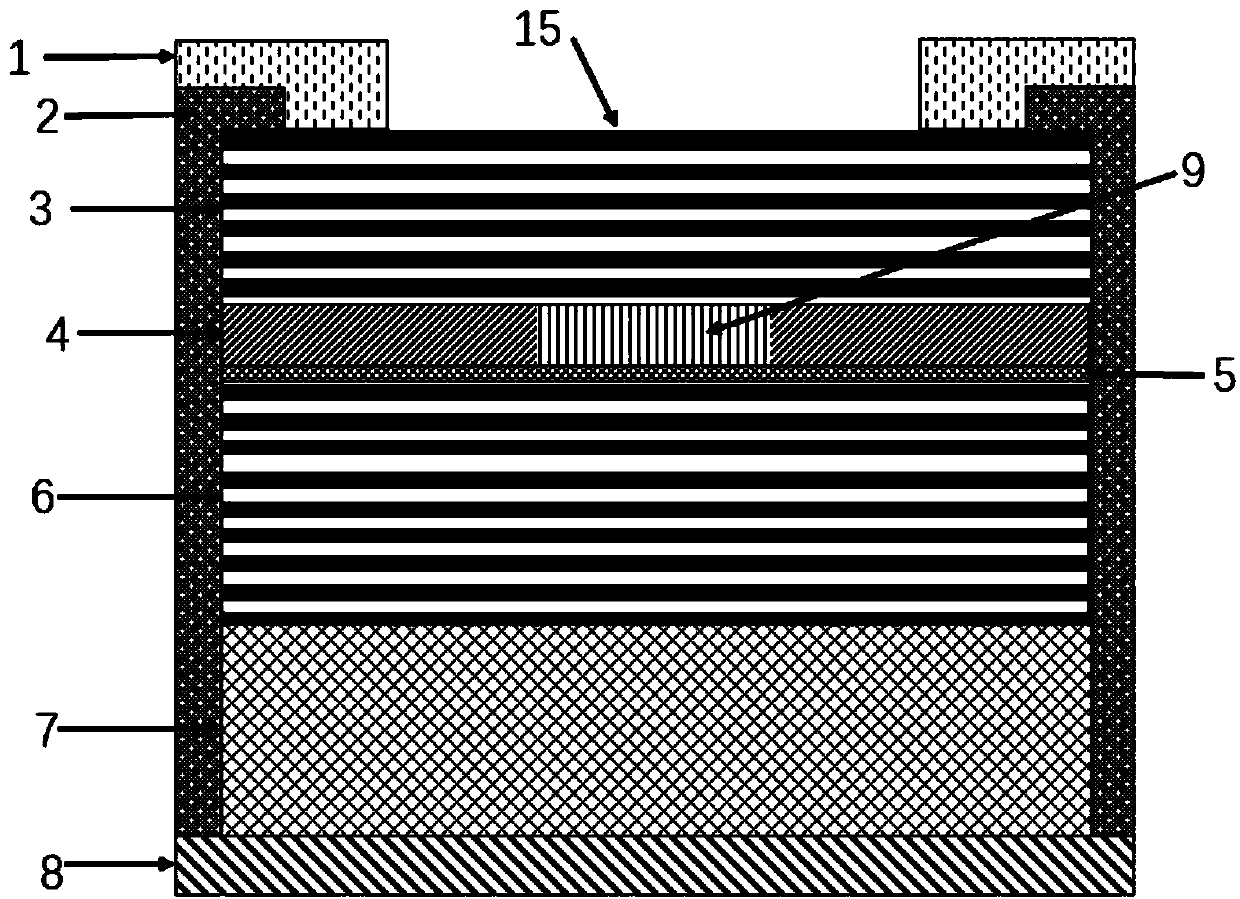
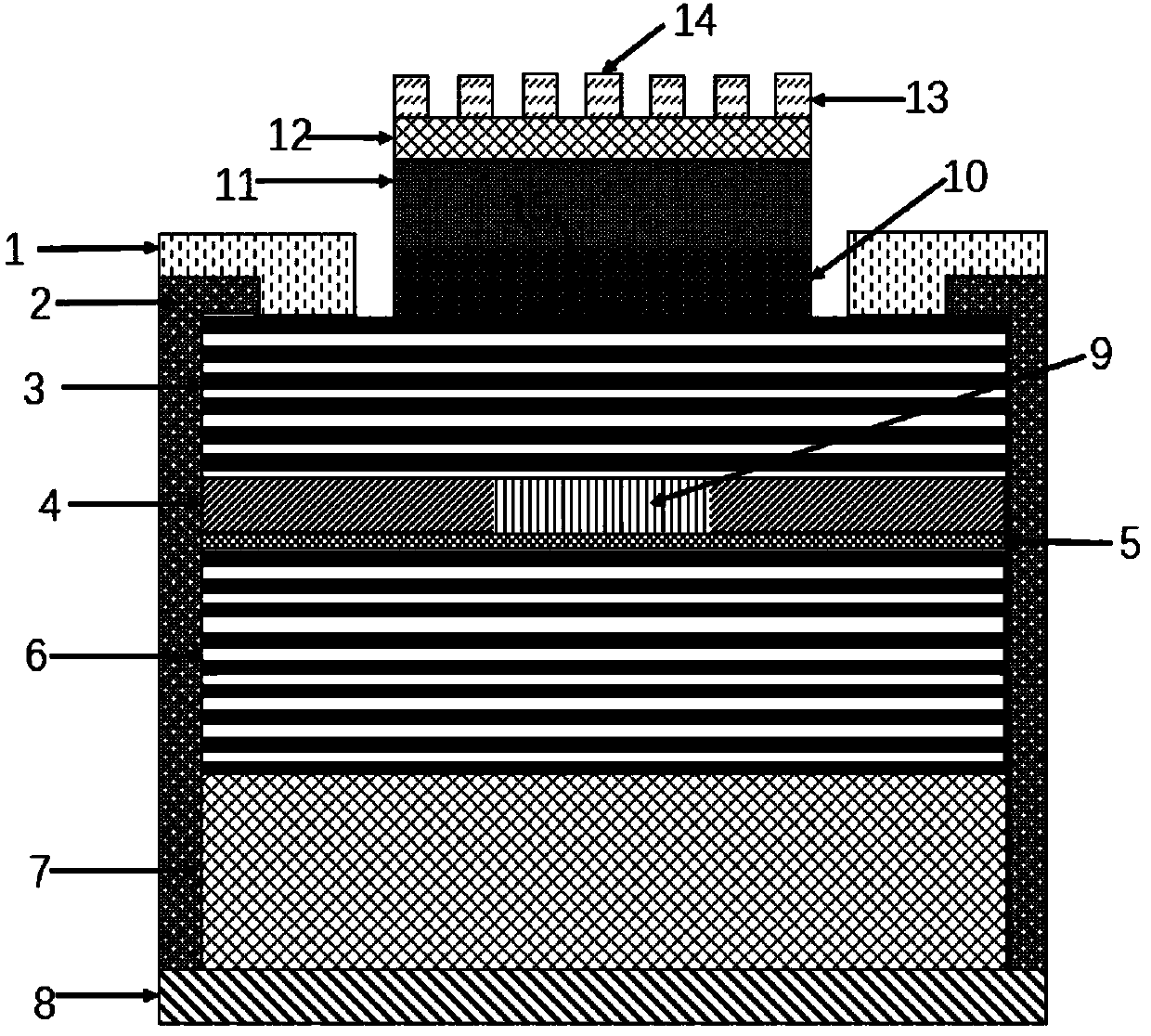
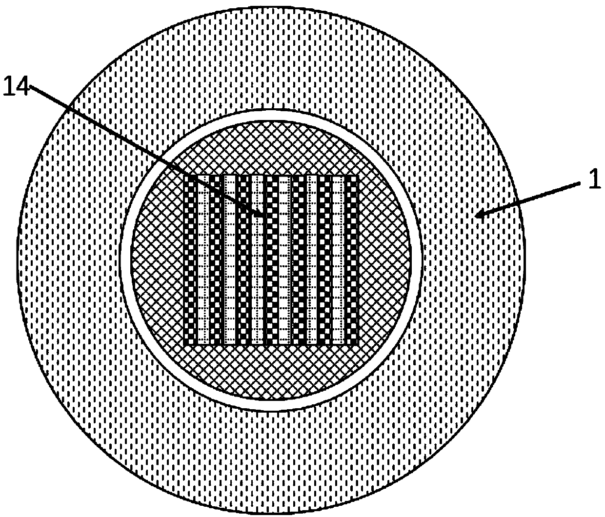
[0020] Such as Figure 1-3 As shown, the 850nm epitaxial wafer is grown by MOCVD, silicon dioxide is deposited by PECVD, the mesa pattern is obtained after photolithography, and the mesa is obtained by ICP etching to expose Al 0.98 Ga 0.02 Oxidation-limited layer (4) of As high-alumina component, current-limited oxidation hole (9) is obtained by wet oxidation, passivation layer (2) is grown by PECVD, light exit hole (15) is obtained after photolithography, and magnetron sputtering is used The P-type metal electrode layer (1) is obtained by sputtering and stripping process, the N-type metal electrode layer (8) is obtained by magnetron sputtering, and the ordinary oxidized vertical cavity surface emitting laser (attached figure 1 ); by plasma chemical vapor deposition, magnetron sputtering or MOCVD and other processes, the dielectric layer is deposited to a common vertical cavity surface emitting laser device to form a phase matching layer (10) and a cavity length matching laye...
PUM
 Abstract
Description
Claims
Application Information


