
A recovery circuit for improving the temperature instability of negative bias voltage of sslc level conversion circuit

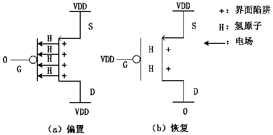
A technology of negative bias temperature and conversion circuit, which is applied in the direction of logic circuit, logic circuit connection/interface arrangement, logic circuit coupling/interface using field effect transistor, etc., which can solve the problem of affecting the performance and service life of PMOS transistors, level conversion Circuit can not work properly and other problems, to achieve the effect of improving static power consumption, suppressing negative drift, and suppressing leakage current

Active Publication Date: 2019-01-15
SUZHOU KUANWEN ELECTRONICS SCI & TECH
View PDF6 Cites 0 Cited by
  • Summary
  • Abstract
  • Description
  • Claims
  • Application Information

AI Technical Summary

Problems solved by technology

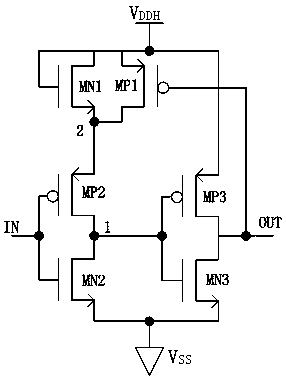
Since the sources of the three PMOS transistors MP1, MP2 and MP3 are connected to a high voltage during normal operation, when the gate is connected to a low level of 0V, there will be a large voltage difference VPP between the gate and the source. Under normal circumstances, the PMOS transistor will experience a more serious NBTI effect during normal operation, which will directly affect the performance and service life of the PMOS transistor, and eventually cause the entire level shifting circuit to fail to work normally.

Method used


Image

  • A recovery circuit for improving the temperature instability of negative bias voltage of sslc level conversion circuit
  • A recovery circuit for improving the temperature instability of negative bias voltage of sslc level conversion circuit
  • A recovery circuit for improving the temperature instability of negative bias voltage of sslc level conversion circuit

Examples


Embodiment Construction

[0023] Hereinafter, the present invention will be described in detail with reference to the accompanying drawings and the embodiments.

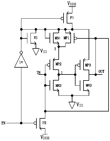
[0024] Reference figure 2 with image 3 As shown, a recovery circuit for improving the negative bias temperature instability of an SSLC level conversion circuit, the circuit includes an SSLC level conversion circuit and an NBTI effect recovery unit;

[0025] The SSLC level conversion circuit includes PMOS transistors MP1, MP2, MP3 and NMOS transistors MN1, MN2, MN3. The sources of MP1 and MP3 are connected, and the gate of MP1 is connected to the drain of MP3 and MN3, respectively. The drain is connected to the source of MP2 and MN1, the gate of MP2 is connected to the gate of MN2, and the drain of MP2 is connected to the drain of MN2 and the gate of MP3, respectively;

[0026] The gate and drain of the MN1 are connected to the source of MP1, and the source of the MN2 is connected to the low-level terminal V SS , The gate of MN2 is connected to t...


PUM


Abstract

The invention discloses a recovery circuit for improving negative bias temperature instability (NBTI) of an SSLC level conversion circuit, which comprises an SSLC level conversion circuit and an NBTI effect recovery unit, wherein the SSLC level conversion circuit comprises PMOS transistors MP1, MP2 and MP3 and NMOS transistors MN1, MN2 and MN3; the NBTI effect recovery unit comprises PMOS transistors P1 and P2, an NMOS transistor N1, an inverter iv and a recovery enabling control end EN; sources of the P1 and the P2 are connected with a high-level end VDDH; the gate of the P1 is connected with the output end of the inverter iv; the gate of the P2 is connected with the recovery enabling control end EN; the drain of the P1 is connected with the source of the MP1; the drain of the P2 is connected with the gate of the MP1; the drain of the N1 is connected with the output end of the inverter iv; the drain of the N1 is connected with the source of the MP1; and the source of the N1 is connected with a low-level end VS. Negative drift and leakage current of PMOS transistor threshold voltage can be effectively restrained, the performance and the reliability of the level conversion circuit are improved, and static power consumption is improved.

Description

Technical field [0001] The invention belongs to the technical field of Flash memory, and relates to a recovery circuit for improving the negative bias temperature instability of an SSLC level conversion circuit. Background technique [0002] With the development of microelectronics technology, especially the rapid development of portable electronic devices such as mobile phones and notebook computers in recent years, the integration of semiconductor memory integrated circuits has become higher and higher, and the requirements for transistor performance have also increased. Therefore, the requirements for transistor reliability have also increased. In the CMOS process, negative gate voltage temperature instability (NBTI) will greatly affect the working stability of PMOS. [0003] The NBTI (negative bias temperature instability) effect occurs in PMOS devices. When the gate of the device is under a negative bias, the saturated drain current Idsat and transconductance Gm of the device...

Claims


Application Information

Patent Timeline
Patent Type & Authority Patents(China)
IPC IPC(8): H03K19/00H03K19/003H03K19/0185
CPCH03K19/0013H03K19/00315H03K19/018557
Inventor 刘世安
Owner SUZHOU KUANWEN ELECTRONICS SCI & TECH
Learn More