Manufacturing method of touch screen, touch screen and display substrate
A production method and touch screen technology, which is applied in the field of touch screen and display substrate, and touch screen production, can solve the problems of damage to the polarizing plate and the formation of electrodes that cannot be touched on the polarizing plate, etc., and achieve a good adhesion effect
- Summary
- Abstract
- Description
- Claims
- Application Information
AI Technical Summary
Problems solved by technology
Method used
Image
Examples
Embodiment 1
[0040] figure 1 A flow chart of the manufacturing method of the touch screen provided by Embodiment 1 of the present invention is shown. see figure 1 , the touch screen manufacturing method provided by Embodiment 1 of the present invention includes the following steps:
[0041] Step 101: attaching the transparent conductive layer on the polarizer through a transfer printing process.
[0042] Step 102: Patterning the transparent conductive layer by patterning process, so that a plurality of touch electrodes are formed on the polarizer to obtain a touch screen.
[0043] In this embodiment, the transparent conductive layer may be made of ITO.
[0044] In this embodiment, the transparent conductive layer is attached to the polarizer through a transfer printing process, which can not only ensure good adhesion between the transparent conductive layer and the polarizer, but also ensure that the polarizer is not damaged. Since the polarizer is generally made of colloidal material,...
Embodiment 2
[0046] Embodiment 2 of the present invention provides an implementation manner of attaching the transparent conductive layer on the polarizer through the transfer printing process in the above step 101 .
[0047] In this example, see figure 2 , the step 101 attaches the transparent conductive layer to the polarizer through a transfer printing process, specifically including:
[0048] Step 101: Attach the transparent conductive layer on the polarizer by applying pressure to the transparent conductive layer under preset heating conditions.
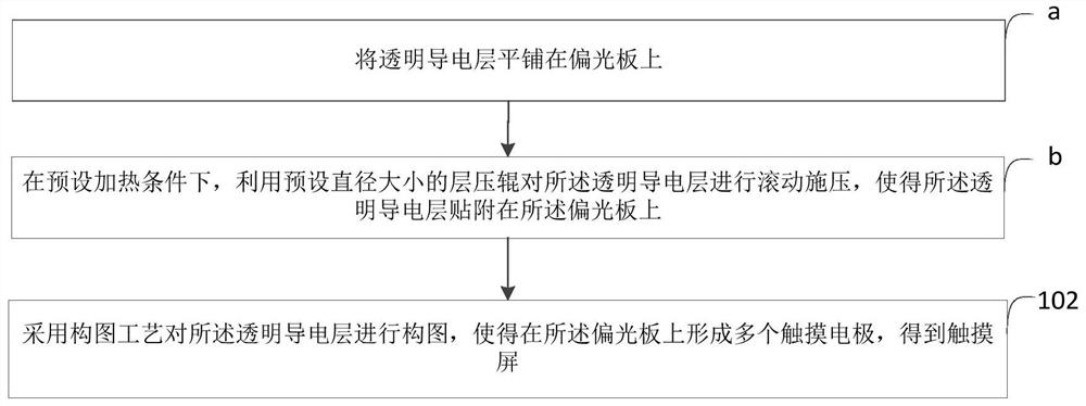
[0049] see image 3 , in this embodiment, a specific implementation method of attaching the transparent conductive layer to the polarizer by applying pressure to the transparent conductive layer under preset heating conditions in step 101 is also given. , including:
[0050] Step a: spread the transparent conductive layer on the polarizer.
[0051] Step b: Rolling and pressing the transparent conductive layer with a lamination roller wi...
Embodiment 3
[0065] In the above-mentioned embodiment 2, an implementation method of attaching the transparent conductive layer to the polarizing plate through the transfer printing process in step 101 has been given, that is, under preset heating conditions, by applying pressure to the transparent conductive layer The transparent conductive layer is pasted on the polarizer.
[0066] In addition, the above-mentioned embodiment 2 also provides an embodiment in which the transparent conductive layer is attached to the polarizer by rolling and applying pressure.
[0067] Different from rolling pressure in the second embodiment, this embodiment provides an implementation manner in which the transparent conductive layer is attached to the polarizer by plane pressure.
[0068] see Figure 5 , in this embodiment, under preset heating conditions, the transparent conductive layer is attached to the polarizer by applying pressure to the transparent conductive layer, specifically including:
[0069...
PUM
 Abstract
Description
Claims
Application Information
 - R&D
- Intellectual Property
- Life Sciences
- Materials
- Tech Scout
- Unparalleled Data Quality
- Higher Quality Content
- 60% Fewer Hallucinations
Browse by: Latest US Patents, China's latest patents, Technical Efficacy Thesaurus, Application Domain, Technology Topic, Popular Technical Reports.
© 2025 PatSnap. All rights reserved.Legal|Privacy policy|Modern Slavery Act Transparency Statement|Sitemap|About US| Contact US: help@patsnap.com


