Source electrode driving module power supply circuit, display panel and display device

A technology of power supply circuit and source drive, applied in static indicators, instruments, etc., can solve the problems of source drive module circuit burnout, AVDD high current, source drive module circuit burnout, etc.

Active Publication Date: 2016-08-10
BOE TECH GRP CO LTD +1
View PDF6 Cites 11 Cited by
  • Summary
  • Abstract
  • Description
  • Claims
  • Application Information

AI Technical Summary

Problems solved by technology

[0002] There is a design flaw in the source driver IC used in the current display device products, that is, the digital working voltage VDD and the analog working voltage AVDD of the two power supply voltages for the source driving module, when VDDAVDD_max, AVDD will generate a large current, causing the circuit of the source driver module to be burned, where VDD_min is the minimum value of the digital working voltage, and AVDD_max is the maximum value of the analog working voltage
[0003] Specifically, the situations that cause the circuit of the source driver module to be burned include: 1. When the display device is turned off, see figure 1 , VDD is powered off, so that VDD
2. When the AVDD power supply of the display device is not converted by VDD, but is powered by an external circuit, if there is a live operation plugging action, or the connector is misaligned, a higher voltage such as VGH will be loaded on the AVDD power supply In the process, the high voltage of AVDD will be caused, which will also cause the circuit of the source driver module to be burned
[0004] Therefore, with the increase in the number of switching on and off of the display device, or the plugging and unplugging actions of live work, etc., the voltage of AVDD increases and excessive current is generated, which causes the circuit of the source driver module to be burned, which has a serious impact on the reliability of the product. influences

Method used


Image

  • Source electrode driving module power supply circuit, display panel and display device
  • Source electrode driving module power supply circuit, display panel and display device
  • Source electrode driving module power supply circuit, display panel and display device

Examples


Embodiment 1

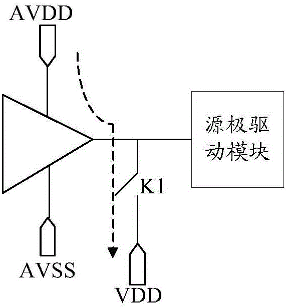
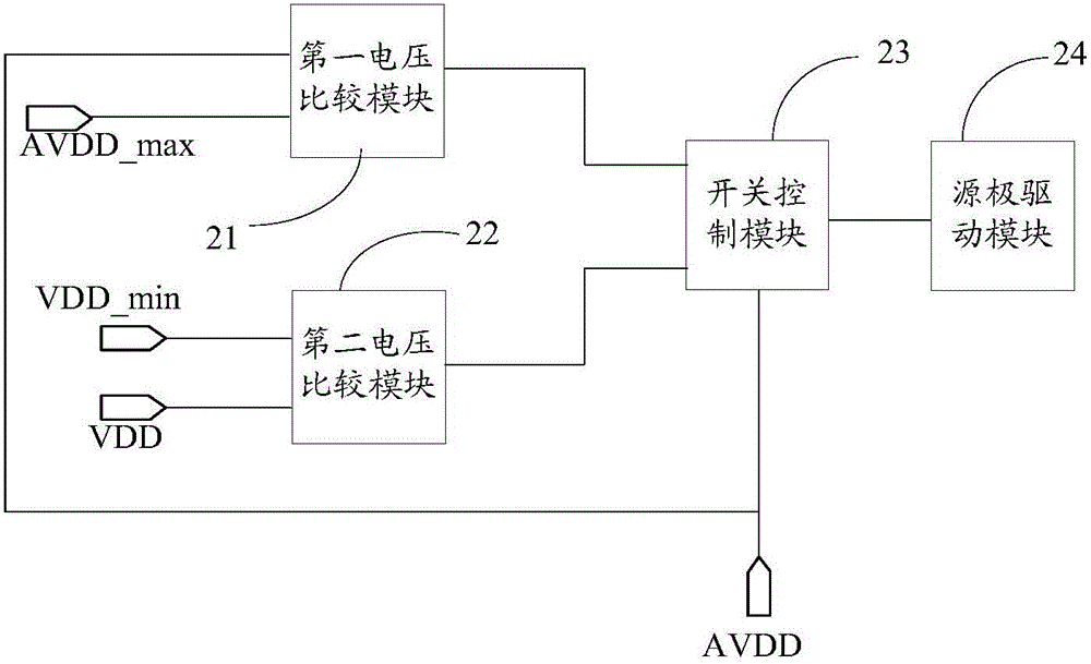
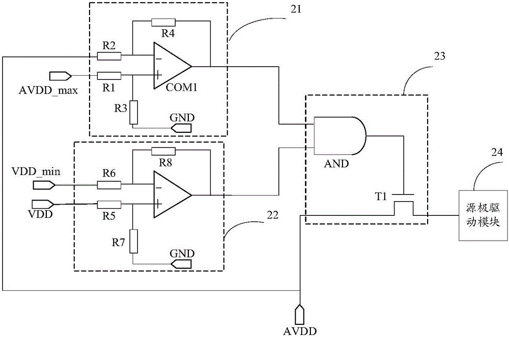
[0095] by Figure 5 The structure of the power supply circuit shown is taken as an example to describe its working process, in which Figure 5 In the power supply circuit shown, the first switching device T1 and the second switching device T2 are both N-type transistors, and each N-type transistor is turned on under the action of a high level and turned off under the action of a low level.

[0096] When AVDD is less than AVDD_max, the first comparator COM1 outputs a high level and supplies it to the first input terminal of the AND gate; when VDD is greater than VDD_min, the second comparator COM2 outputs a high level and supplies it to the second input of the AND gate At the same time, the AND gate outputs a high level, then the first switching device T1 and the second switching device T2 are turned on, and both the digital voltage signal VDD and the analog voltage signal AVDD are input to the source drive module, so when the switch control module outputs digital The voltage ...

Embodiment 2

[0102] by Figure 6 The structure of the power supply circuit shown is taken as an example to describe its working process, in which Figure 6 In the power supply circuit shown, the AND gate is set as a NAND gate, the first switching device T1 and the second switching device T2 are both P-type transistors, each P-type transistor is turned on under the action of a low level, and is turned on at a high level cut off under action.

[0103] When AVDD is less than AVDD_max, the first comparator COM1 outputs a high level and provides it to the first input terminal of the NAND gate. When VDD is greater than VDD_min, the second comparator COM2 outputs a high level and provides it to the first input terminal of the NAND gate. At the two input terminals, at the same time, the NAND gate outputs a low level, then the first switching device T1 and the second switching device T2 are turned on, and both the digital voltage signal VDD and the analog voltage signal AVDD are input to the sourc...


PUM


Abstract

The invention discloses a source electrode driving module power supply circuit, a display panel and a display device, and aims at avoiding the adverse phenomena of burnout of a source electrode driving module due to oversized or undersized power supply voltage of the power supply circuit. The power supply circuit comprises a first voltage comparison module, a second voltage comparison module and a switch control module. The first voltage comparison module is used for comparing the size of an analog voltage signal and reference voltage of analog voltage. When the analog voltage signal is determined to be greater than or equal to the reference voltage of the analog voltage, a first signal is outputted to the switch control module. The second voltage comparison module is used for comparing the size of a digital voltage signal and reference voltage of digital voltage. When the digital voltage signal is determined to be less than or equal to the reference voltage of the digital voltage, a third signal is outputted to the switch control module. The switch control module is used for stopping outputting of the analog voltage signal when the switch control module receives the first signal or the third signal.

Description

technical field [0001] The present invention relates to the field of display technology, in particular to a power supply circuit of a source drive module, a display panel and a display device. Background technique [0002] There is a design flaw in the source driver IC used in the current display device products, that is, the digital working voltage VDD and the analog working voltage AVDD of the two power supply voltages for the source driving module, when VDD<VDD_min, Or when AVDD>AVDD_max, AVDD will generate a large current, causing the circuit of the source driver module to be burned, where VDD_min is the minimum value of the digital working voltage, and AVDD_max is the maximum value of the analog working voltage. [0003] Specifically, the situations that cause the circuit of the source driver module to be burned include: 1. When the display device is turned off, see figure 1 , VDD is powered off, so that VDD<VDD_min, at this time switch K1 is closed, and each ...

Claims


Application Information

Patent Timeline
Patent Type & Authority Applications(China)
IPC IPC(8): G09G3/20
CPCG09G3/2077
Inventor 张郑欣徐帅
Owner BOE TECH GRP CO LTD
Why Eureka
Try Eureka