A kind of broadband wave-absorbing magnetic thin film and its preparation method

A magnetic thin film and broadband technology, applied in the field of broadband absorbing magnetic thin film and its preparation, can solve difficulties, reduce film absorption effect, increase cost and other problems, and achieve the effect of low cost and simple and easy preparation process

Active Publication Date: 2018-05-18
UNIV OF ELECTRONICS SCI & TECH OF CHINA
View PDF4 Cites 0 Cited by
  • Summary
  • Abstract
  • Description
  • Claims
  • Application Information

AI Technical Summary

Problems solved by technology

[0004] For a single-layer film, in order to realize the absorption of electromagnetic waves in a wider frequency band, theoretically speaking, the damping factor of the film magnetic moment resonance can be increased to broaden the resonant absorption frequency band of the film, but it is difficult to simply control the damping factor Yes, too much damping will also reduce the absorption effect of the film
In fact, the post-annealing treatment of the film can form multiple magnetic phases in the film, which can also broaden the absorption band of the film, but the subsequent treatment will increase the cost accordingly, and the annealing treatment cannot be used in a large area in the industry.

Method used


Image

  • A kind of broadband wave-absorbing magnetic thin film and its preparation method
  • A kind of broadband wave-absorbing magnetic thin film and its preparation method
  • A kind of broadband wave-absorbing magnetic thin film and its preparation method

Examples


Embodiment 1

[0024] Embodiment 1: the preparation of the broadband absorbing magnetic thin film that thickness is 45nm

[0025] Step 1. The Si(111) substrate with a size of 15mm×5mm×0.5mm was ultrasonically cleaned with acetone for 5 minutes, ultrasonically cleaned with absolute ethanol for 5 minutes, and then rinsed with deionized water for 5 times. After blowing off the deionized water on the surface of the sheet with compressed air, place it on a heating platform and dry it at 170°C for ten minutes until moisture drying.

[0026] Step 2. Place the Si substrate dried in step 1 on the glue-spinning machine, set the speed at 3000 rpm, use the negative glue AZ5214, and drip the glue. After the glue is finished, start to throw the glue, and form a 1μm thick layer on the Si substrate. film.

[0027] Step 3. Place the Si substrate after the glue-spinning in step 2 on a heating platform and bake at 100° C. for 60 seconds.

[0028] Step 4, install the mask plate in the exposure machine, place ...

Embodiment 2

[0033] Embodiment 2: the preparation of the broadband absorbing magnetic thin film that thickness is 75nm

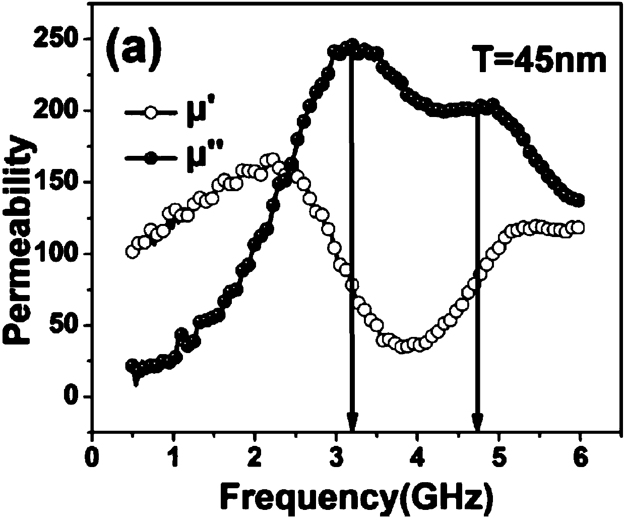
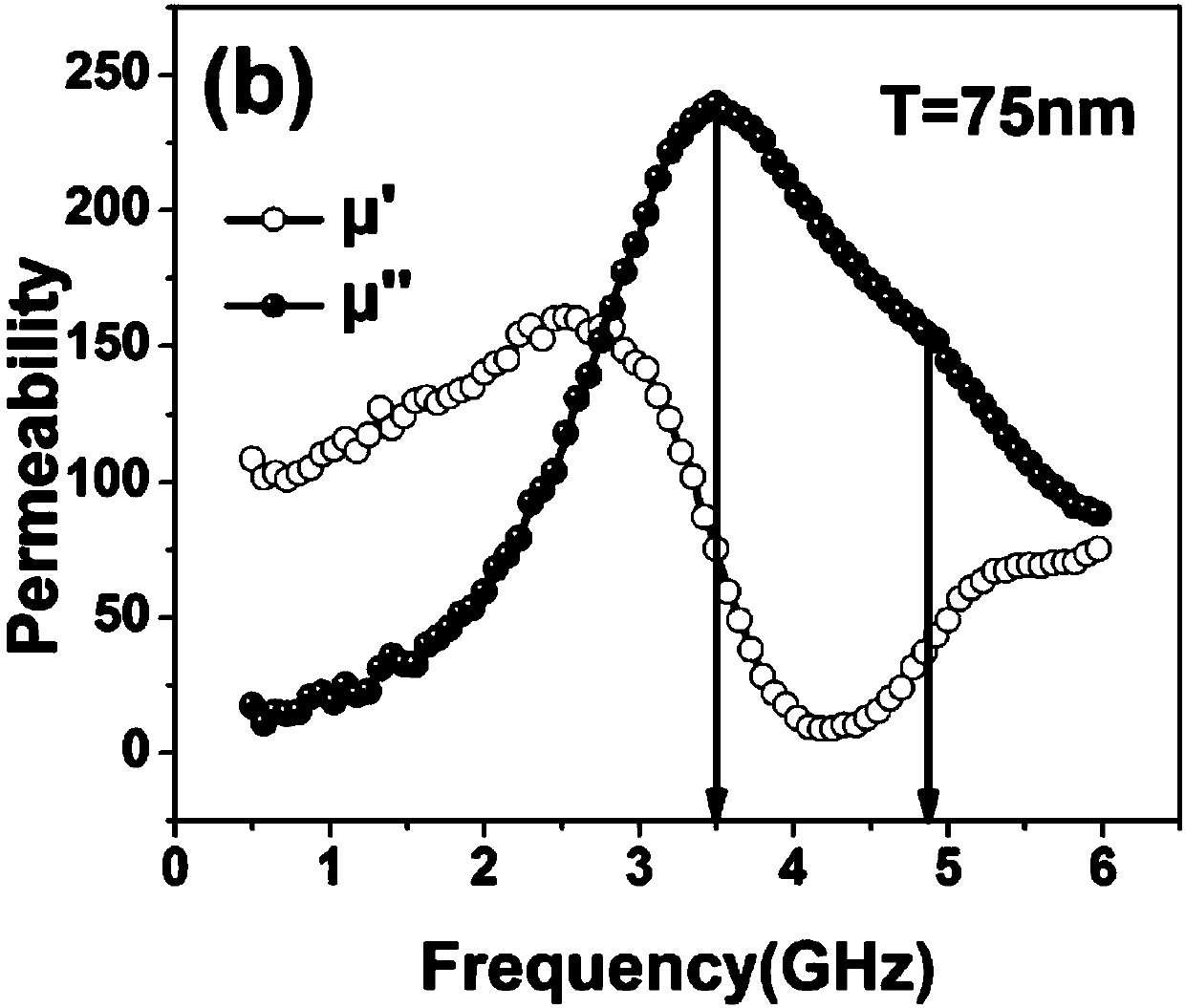
[0034] The other preparation conditions are the same as in Example 1, but the sputtering time is extended to 5 minutes and 38 seconds, the Si substrate is taken out, placed in acetone for ultrasonic cleaning, then rinsed with alcohol, and the surface is dried with an ear cleaning ball to obtain the thickness 75nm broadband absorbing magnetic film. Test the thin film that above-mentioned embodiment makes through short circuit microstrip line method and obtain as follows figure 2 and image 3 From the magnetic spectrum test charts of the two thin films shown, it can be seen that the resonance peak of the 45nm thin film combines the resonance peaks of each strip thin film, the half maximum width is 3.5 GHz, and the resonance peak is obviously broadened and double-peaked. For a film with a thickness of 75nm, it can be seen that the resonant peak has a bulge at 4.8GHz, and...


PUM

PropertyMeasurementUnit
widthaaaaaaaaaa
widthaaaaaaaaaa
thicknessaaaaaaaaaa

Abstract

The invention belongs to the technical field of magnetic material preparation, and in particular relates to a broadband wave-absorbing magnetic thin film and a preparation method thereof. The broadband wave-absorbing magnetic film is a film that is periodically arranged on a substrate. The basic unit is composed of more than two strip films with different widths. The width of the strip films is 1 μm-30 μm. The gap width is 1μm-10μm, and the thickness is 20-200nm. The arrangement period is that the basic units are arranged sequentially along the short axis direction of the strip film, and the material is an iron-cobalt-based alloy material. The present invention combines strip films of different widths with strip gaps of the same width, and blocks the coupling effect between the films through the gaps, so that the resonance peaks corresponding to different strip films can be effectively superimposed together to achieve the purpose of broadening the resonance frequency band of the film. Purpose. The broadband wave-absorbing magnetic thin film prepared by the invention has high-frequency and broadband wave-absorbing properties, the preparation process is simple and easy to implement, and the cost is low.

Description

technical field [0001] The invention belongs to the technical field of magnetic material preparation, and in particular relates to a broadband wave-absorbing magnetic thin film and a preparation method thereof, which can be applied to thin-film electromagnetic interference suppressors and other devices. Background technique [0002] With the development of radio communication technology and the high integration of electronic equipment, the high-density and wide-spectrum electromagnetic signals generated by integrated electronic devices in operation fill the entire space, forming a complex electromagnetic environment, which requires electronic equipment and power supplies to be in each The frequency bands have good electromagnetic compatibility, which brings a series of challenges to the anti-electromagnetic interference technology. [0003] High-frequency magnetic film has excellent electromagnetic loss effect at high frequency, and its thin and light features make it have a...

Claims


Application Information

Patent Timeline
Patent Type & Authority Patents(China)
IPC IPC(8): H01F41/14H01F10/16C23C14/04C23C14/14
CPCC23C14/042C23C14/14H01F10/16H01F41/14
Inventor 张丽李梦高丽娜朱文斌郑菡雨王昕邓龙江谢建良梁迪飞周佩珩陆海鹏
Owner UNIV OF ELECTRONICS SCI & TECH OF CHINA
Why Eureka
Try Eureka