Broadband wave-absorbing magnetic film and preparation method thereof
A magnetic film and broadband technology, applied in the field of broadband wave-absorbing magnetic film and its preparation, can solve problems such as difficulty, reduce film absorption effect, increase cost, etc., and achieve the effects of low cost, simple and easy-to-implement preparation process
- Summary
- Abstract
- Description
- Claims
- Application Information
AI Technical Summary
Problems solved by technology
Method used
Image
Examples
Embodiment 1
[0024] Embodiment 1: the preparation of the broadband absorbing magnetic thin film that thickness is 45nm
[0025] Step 1. The Si(111) substrate with a size of 15mm×5mm×0.5mm was ultrasonically cleaned with acetone for 5 minutes, ultrasonically cleaned with absolute ethanol for 5 minutes, and then rinsed with deionized water for 5 times. After blowing off the deionized water on the surface of the sheet with compressed air, place it on a heating platform and dry it at 170°C for ten minutes until moisture drying.
[0026] Step 2. Place the Si substrate dried in step 1 on the glue-spinning machine, set the speed at 3000 rpm, use the negative glue AZ5214, and drip the glue. After the glue is finished, start to throw the glue, and form a 1μm thick layer on the Si substrate. film.
[0027] Step 3. Place the Si substrate after the glue-spinning in step 2 on a heating platform and bake at 100° C. for 60 seconds.
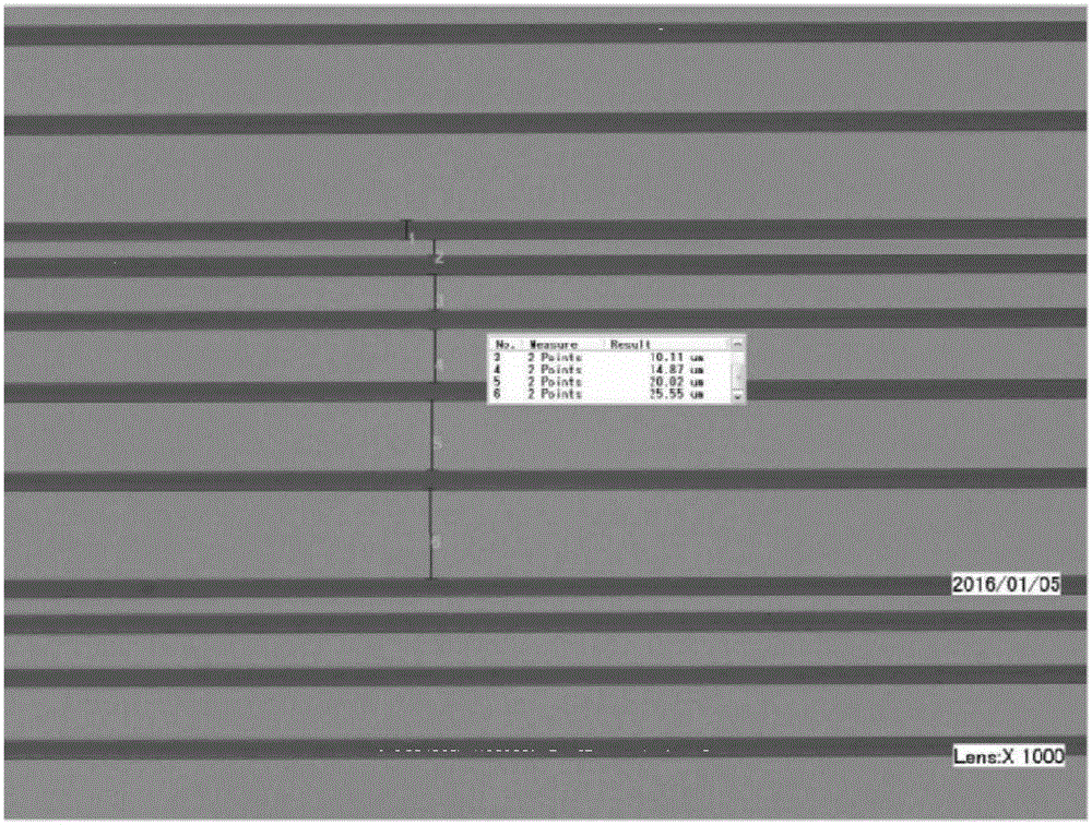
[0028] Step 4, install the mask plate in the exposure machine, place ...
Embodiment 2
[0033] Embodiment 2: the preparation of the broadband absorbing magnetic thin film that thickness is 75nm
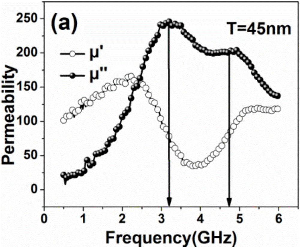
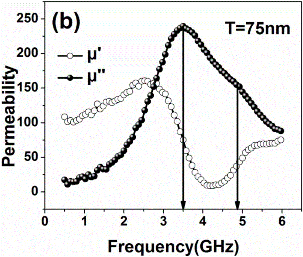
[0034] The other preparation conditions are the same as in Example 1, but the sputtering time is extended to 5 minutes and 38 seconds, the Si substrate is taken out, placed in acetone for ultrasonic cleaning, then rinsed with alcohol, and the surface is dried with an ear cleaning ball to obtain the thickness 75nm broadband absorbing magnetic film. Test the thin film that above-mentioned embodiment makes through short circuit microstrip line method and obtain as follows figure 2 and image 3 From the magnetic spectrum test charts of the two thin films shown, it can be seen that the resonance peak of the 45nm thin film combines the resonance peaks of each strip thin film, the half maximum width is 3.5 GHz, and the resonance peak is obviously broadened and double-peaked. For a film with a thickness of 75nm, it can be seen that the resonant peak has a bulge at 4.8GHz, and...
PUM
| Property | Measurement | Unit |
|---|---|---|
| width | aaaaa | aaaaa |
| width | aaaaa | aaaaa |
| thickness | aaaaa | aaaaa |
Abstract
Description
Claims
Application Information


