Supercharge Your Innovation With Domain-Expert AI Agents!

Light emitting semiconductor component comprising an absorptive layer

A semiconductor and device technology, applied in the field of semiconductor devices, can solve problems such as difficult to detect radiation and drop, and achieve the effect of effective absorption

Active Publication Date: 2016-08-10
OSRAM OPTO SEMICONDUCTORS GMBH & CO OHG
View PDF5 Cites 0 Cited by
  • Summary
  • Abstract
  • Description
  • Claims
  • Application Information

AI Technical Summary

Problems solved by technology

However, the sensitivity of conventional silicon detectors drops for wavelengths above 850 nm, making it difficult to detect radiation above this wavelength

Method used


Image

  • Light emitting semiconductor component comprising an absorptive layer
  • Light emitting semiconductor component comprising an absorptive layer
  • Light emitting semiconductor component comprising an absorptive layer

Examples


Embodiment Construction

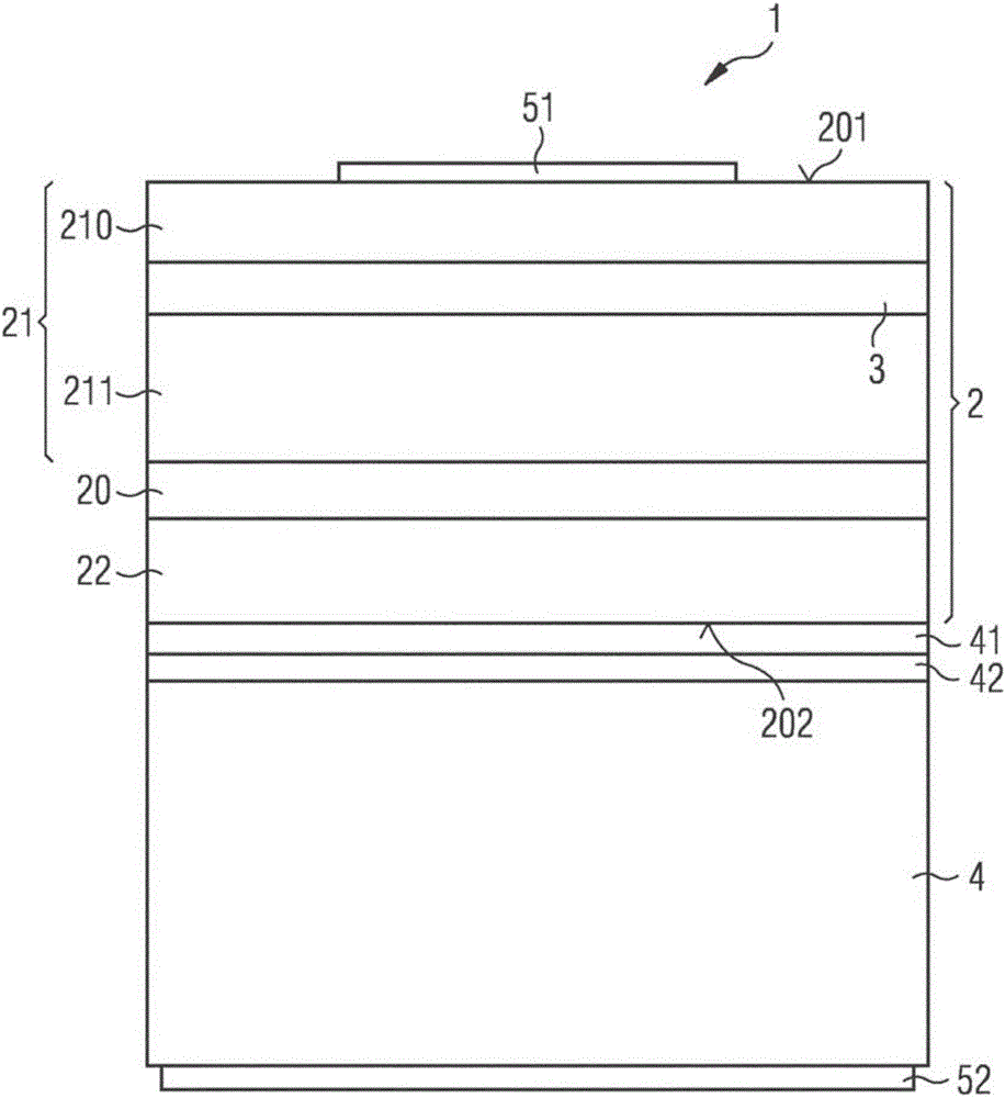
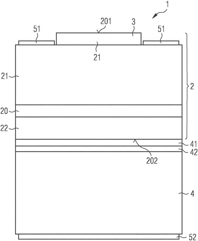
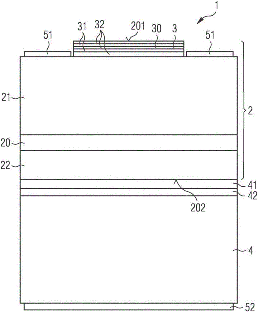
[0037] exist figure 1 A first exemplary embodiment of a radiation-emitting semiconductor component is shown in . The semiconductor component 1 comprises a semiconductor body having a semiconductor layer sequence 2 . The semiconductor body 2 extends between a radiation exit surface 201 and a rear side 202 opposite the radiation exit surface in a vertical direction extending perpendicularly to a main plane of extent of the semiconductor layers of the semiconductor body. The semiconductor body has a semiconductor material of the semiconductor layer sequence, in particular an epitaxially deposited semiconductor material, only between the radiation exit surface and the rear side.

[0038] The semiconductor body 2 also includes an active region 20 provided for generating radiation in the near infrared. The active region 20 is preferably designed to generate radiation with a peak wavelength between 830 nm and 920 nm, particularly preferably between 830 nm and 870 nm, for example 8...


PUM


Abstract

Disclosed is a radiation-emitting semiconductor component (1) comprising a semiconductor element that has a succession of semiconductor layers (2) which includes an active region (20) for generating radiation having a peak wavelength in the near-infrared spectral range as well as an absorptive region (3). The absorptive region at least partially absorbs a short-wave portion of the radiation that has a maximum wavelength which is shorter than the peak wavelength.

Description

technical field [0001] The invention relates to a radiation-emitting semiconductor component. Background technique [0002] For various applications, radiation-emitting semiconductor components, such as light-emitting diodes, are desirable which emit radiation in the infrared spectral range. It has been found that components that emit radiation in the near infrared, for example at an emission wavelength of 850 nm, can have short-wavelength radiation fractions that can still be perceived by the human eye. In order to avoid such radiation fractions, the peak wavelength of the emitted radiation is shifted towards higher wavelengths. However, the sensitivity of conventional silicon detectors drops for wavelengths above 850 nm, making detection of radiation above this wavelength difficult. Contents of the invention [0003] The object of the present invention is to provide a semiconductor component whose emitted radiation is easily detectable and at the same time imperceptibl...

Claims


Application Information

Patent Timeline
Patent Type & Authority Applications(China)
IPC IPC(8): H01L33/02H01L33/30H01L33/44H01S5/343
CPCH01L33/02H01L33/30H01L33/44H01L33/50H01L33/04H01L33/06H01L33/36H01L33/58H01L33/60H01L33/62
Inventor 伊瓦尔·通林彼得鲁斯·松德格伦
Owner OSRAM OPTO SEMICONDUCTORS GMBH & CO OHG
Features
  • R&D
  • Intellectual Property
  • Life Sciences
  • Materials
  • Tech Scout
  • Unparalleled Data Quality
  • Higher Quality Content
  • 60% Fewer Hallucinations
Learn More