Polycrystalline silicon furnace tube deposition thickness monitoring device and method

A furnace tube deposition and monitoring device technology, applied in gaseous chemical plating, coating, electrical components, etc., can solve the problems of inconsistent film thickness on the wafer surface, polysilicon film thickness difference, abnormal monitoring data, etc., to avoid film Inconsistent thickness, reducing monitoring costs, and increasing the number of placements

Active Publication Date: 2016-08-17
SHANGHAI HUAHONG GRACE SEMICON MFG CORP
View PDF5 Cites 11 Cited by
  • Summary
  • Abstract
  • Description
  • Claims
  • Application Information

AI Technical Summary

Problems solved by technology

[0004] Due to the presence of a loading effect in the polysilicon furnace tube process, the polysilicon formed on the surface of the product wafer 20 immediately below the top control sheet TOP C / W and the product wafer 20 immediately below the middle control sheet CTR C / W The thickness is lower than the thickness of polysilicon on the surface of the product wafer in other positions. The possible reason for this difference in thickness is that the back of the top control chip TOP C / W and the back of the middle control chip CTR C / W are compared with their upper surface. There are differences in absorption and reflection, so that the product wafer 20 immediately below the top control plate TOP C / W and the product wafer 20 surface immediately below the middle control plate CTR C / W have different reactant gas concentrations than other positions , the degree of reaction is different, and eventually there is a large difference in polysilicon film thickness between the product wafers in the two places and the product wafers in the same chamber, causing abnormal monitoring data
When subsequent polysilicon etching is performed on the product wafer on the wafer boat, the dryness of the polysilicon film on the surface of the product wafer 20 immediately below the top control sheet TOP C / W and the product wafer 20 immediately below the middle control sheet CTR C / W The dry etching rate of the polysilicon film on the surface of the wafer at other positions is also faster than that of the dry etching rate, which is easy to form such as Figure 1B The pit defects (pits) shown, make the yield of the product drop
[0005] Therefore, there is a need for a polysilicon furnace tube deposition film thickness monitoring device and method, which can avoid the problem of inconsistent film thickness on the surface of the product wafer, and at the same time ensure the authenticity and stability of the monitoring data of the control film, and improve the product yield rate.

Method used


Image

  • Polycrystalline silicon furnace tube deposition thickness monitoring device and method
  • Polycrystalline silicon furnace tube deposition thickness monitoring device and method
  • Polycrystalline silicon furnace tube deposition thickness monitoring device and method

Examples


Embodiment 1

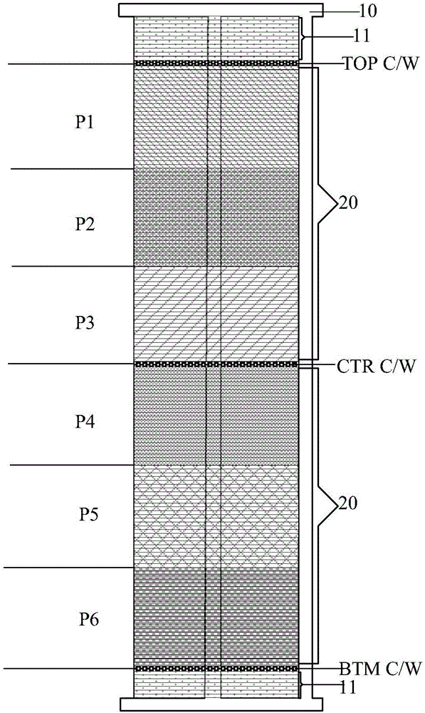
[0035] Please refer to figure 2 , the present embodiment proposes a polysilicon furnace tube deposition film thickness monitoring device, including: a crystal boat 10, a top control chip TOP C / W, a middle control chip CTR C / W, a bottom control chip BTM C / W and A number of product wafers 20 to be polysilicon deposited. Wherein, the top of the wafer boat 10 is loaded with the top control chip TOP C / W, the middle is loaded with the middle control chip CTR C / W, the bottom is loaded with the bottom control chip BTMC / W, and the product to be polysilicon deposited Wafers 20 correspondingly fill the wafer boat loading areas P1, P2, P3 between the top control plate TOP C / W and the middle control plate CTR C / W and the middle control plate CTRC / W and the middle control plate CTR C / W In the boat loading areas P4, P5, and P6 between the bottom control plate BTM C / W, the surfaces of the top control plate TOP C / W and the middle control plate CTR C / W are all annealed, and the annealing trea...

Embodiment 2

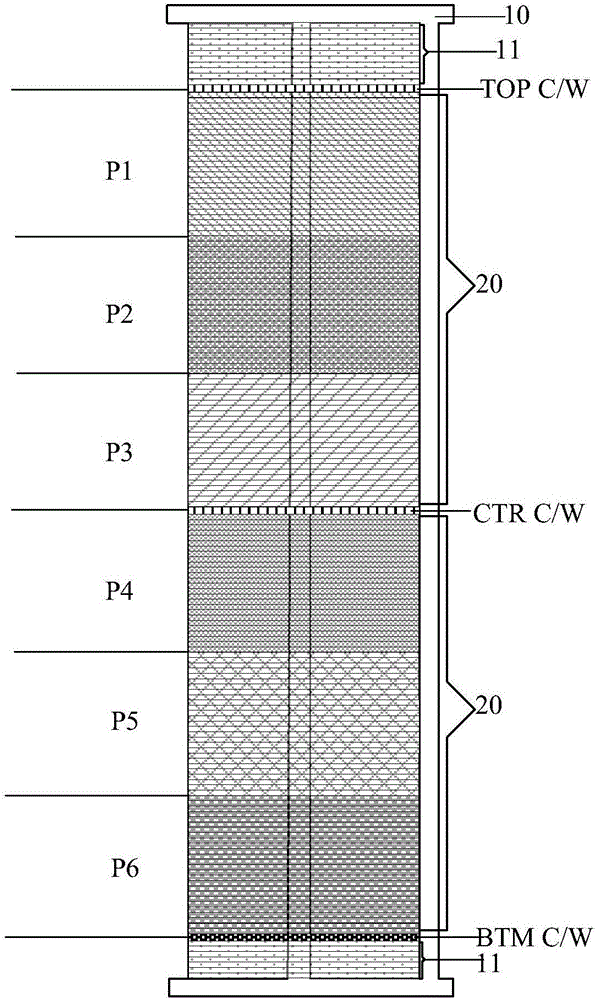
[0045] Please refer to image 3 , the present invention proposes a polysilicon furnace tube deposition film thickness monitoring device, comprising: a crystal boat 10, an upper top control chip TOP C / W1, a lower top control chip TOP C / W2, a middle control chip CTR C / W, a Bottom control chip BTM C / W and several product wafers 20 to be polysilicon deposited. Wherein, the top of the wafer boat 10 is loaded with the upper top control sheet TOP C / W1 and the lower top control sheet C / W2, and the upper top control sheet TOPC / W1 and the lower top control sheet TOP C / W2 are placed next to each other, and the middle part is loaded with all The middle control piece CTR C / W, the bottom control piece BTM C / W is loaded on the bottom, and the product wafer 20 to be polysilicon deposited is correspondingly filled in the lower top control piece TOP C / W2 and the middle control piece In the boat loading areas P1, P2, P3 between the plates CTR C / W and in the wafer loading areas P4, P5, P6 betwee...

Embodiment 3

[0052] Please refer to Figure 4 , the present invention proposes a polysilicon furnace tube deposition film thickness monitoring device, comprising: a crystal boat 10, a top control chip TOP C / W, an upper middle control chip CTR C / W1, a lower middle control chip CTR C / W2, a bottom Control the BTM C / W and several product wafers 20 to be polysilicon deposited. Wherein, the top of the wafer boat 10 is loaded with the top control sheet TOP C / W, the middle is loaded with the upper middle control sheet CTR C / W1, the lower middle control sheet CTR C / W2, and the upper middle control sheet CTR C / W1, The lower middle control piece CTR C / W2 is placed next to each other, and the bottom control piece BTM C / W is loaded on the bottom, and the product wafer 20 to be deposited with polysilicon is correspondingly filled in the top control piece TOP C / W and the upper control piece BTM C / W. The wafer boat loading areas P1, P2, P3 between the middle control plate CTR C / W1 and the wafer boat load...


PUM


Abstract

The invention provides a polycrystalline silicon furnace tube deposited film thickness monitoring device and method. A top control wafer and a middle control wafer can be replaced with control wafers of which the surfaces are subjected to annealing treatment in an existing three control wafer monitoring mode, and the problem that film thicknesses of wafer surfaces of a product are inconsistent can be avoided; meanwhile, the authenticity and stability of control wafer monitoring data are guaranteed, and the product yield is increased.

Description

technical field [0001] The invention relates to the field of semiconductor manufacturing, in particular to a device and method for monitoring the deposition thickness of a polysilicon furnace tube. Background technique [0002] As an important semiconductor thin film material, polysilicon thin film has already attracted people's attention, and it has been widely used in the manufacture of integrated circuits and various electronic devices. , is an ideal structural layer material, and is especially widely used as the basic structural material in microelectromechanical systems (MEMS). [0003] In the prior art, the polysilicon deposition in the semiconductor structure is usually carried out using a vertical furnace tube (Poly Furnace) for low-pressure chemical vapor deposition, and the furnace tube process is different from other monolithic operations in that it is a batch operation, that is, There are multiple batches of product wafers operating in the furnace tube at the sa...

Claims


Application Information

Patent Timeline
Patent Type & Authority Applications(China)
IPC IPC(8): H01L21/66C23C16/44
CPCC23C16/44H01L22/12H01L22/34
Inventor 徐涛陈宏王卉曹子贵梁肖陈广伦
Owner SHANGHAI HUAHONG GRACE SEMICON MFG CORP
Why Eureka
Try Eureka