
An integrated detection mechanism for detection, sorting and sorting of chip components

A detection mechanism and component technology, which is applied in the field of chip component detection and sorting integrated detection mechanism, can solve the problems of low detection efficiency, occupying time, non-stop, etc., and achieve the effects of improving detection efficiency, comprehensive judgment, and avoiding damage

Active Publication Date: 2018-04-10
GUILIN UNIV OF ELECTRONIC TECH
View PDF9 Cites 0 Cited by
  • Summary
  • Abstract
  • Description
  • Claims
  • Application Information

AI Technical Summary

Problems solved by technology

However, the mechanism itself cannot arrange the piles of scattered components, and if the components are arranged closely, some components may stand upright or even turn over when the stopper rod distributes materials.
[0005] Taiwan patent TWI372135 [testing device of electronic component testing and sorting machine], its main purpose is also in order to shorten the waiting time of testing device, this invention has utilized two retrieving devices, carries out retrieving in turn, to reduce the stand-by time of testing station, but It will also take a certain amount of time when the two reclaimers switch
With the increasingly higher requirements for the detection speed of electronic components and the limitation of camera exposure time, the technical means contained in the above patents cannot meet the requirements for efficient and fast testing of bulk electronic components.
[0006] Both of the above two solutions improve the low efficiency of the traditional one-by-one picking method by changing the picking method, but they still cannot achieve non-stop testing, and both need to add an additional component arrangement machine before testing
At the same time, it cannot solve the problems of low detection efficiency and few integrated functions of existing related devices

Method used


Image

  • An integrated detection mechanism for detection, sorting and sorting of chip components
  • An integrated detection mechanism for detection, sorting and sorting of chip components
  • An integrated detection mechanism for detection, sorting and sorting of chip components

Examples


Embodiment 2

[0049] Such as Figure 7 , 8 As shown in 11 and 11, embodiment 2 is basically the same as embodiment 1, only the end of the outer layer detection mechanism and the screening mechanism are different, and only the differences are described here.

[0050] The conveyor belt 49 is completely positioned on the base 4, and its end (outside end) protrudes slightly from the outer edge of the base 4. Simultaneously, the beating mechanism of present embodiment screening mechanism 3 hangs on the outside of conveyer belt 18 ends.

[0051] The output shaft of the screening motor 16 is connected to the eccentric wheel 43, the eccentric wheel overcoat has a connecting rod 44, the connecting rod 44 is connected to the striking rod 45, and the striking rod 45 is a rectangular frame, the lower surface of which is the striking part, and the left and right sides are Embedded in the striking slot 46, it can move vertically along the slot 46.

[0052] When the component is delivered to the outer ...


PUM


Abstract

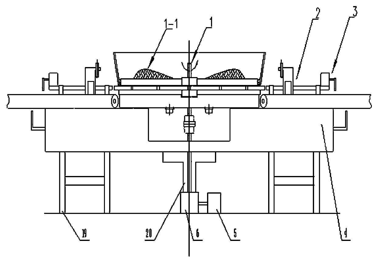
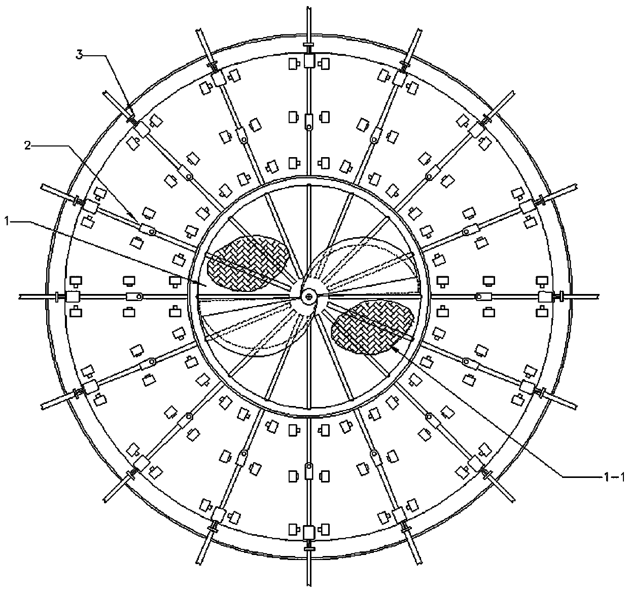
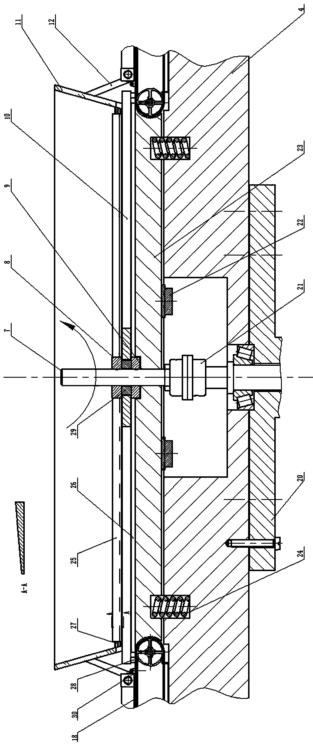
The invention discloses an integrated detection mechanism for chip component detection and separation. The integrated detection mechanism comprises three major parts, namely an inner layer arrangement mechanism, an outer layer detection mechanism and a screening mechanism; the an inner layer arrangement mechanism, the outer layer detection mechanism and the screening mechanism are all arranged on an annular base, the base is supported by a base support and a first central main shaft sleeve, and the first shaft sleeve presses a speed change device. Elements which are arranged well can be output and detected from multiple tracks at the same time only by pouring the scattered elements from a middle feeding position. The whole mechanism runs smoothly, and compared with traditional detection mechanisms, detection efficiency is greatly improved. Meanwhile, an industrial camera and an ultrasonic fault detection head are comprehensively applied for detection, more items can be detected, element quality is judged more completely, and the misjudgment rate is lower. The element detection process does not need to be stopped, and damage to elements caused when material picking and discharging are conducted through a material picker is avoided. In addition, aggregation of unqualified elements can be achieved.

Description

technical field [0001] The invention relates to the technical field of chip component detection, in particular to an integrated detection mechanism for chip component detection, sorting and sorting. Background technique [0002] With the rapid development of the information industry revolution, the complexity of electronic devices and systems is increasing, and the number of electronic components required is also increasing. From the perspective of reliability, the quality requirements for electronic components are also getting higher and higher. [0003] SMD components are currently the most important components in electronic equipment, and their quality screening plays an important role in improving the reliability of electronic equipment. At this stage, the machines used for online component detection are mainly attached to the braiding machine, and the components need to be placed on a transparent detection platform during the detection, and after the detection is compl...

Claims


Application Information

Patent Timeline
Patent Type & Authority Patents(China)
IPC IPC(8): B07C5/02B07C5/34B07C5/36
CPCB07C5/02B07C5/34B07C5/36B07C2301/0008
Inventor 高兴宇邓仕超高阳彭泽令
Owner GUILIN UNIV OF ELECTRONIC TECH
Learn More