Unlock instant, AI-driven research and patent intelligence for your innovation.

Terminal connecting structure and semiconductor device

A technology of terminal connection and convex terminal, which is applied in the direction of connection, coupling device, vehicle connector, etc., can solve the problem of being easily affected by vibration, and achieve the effect of ensuring durability

Inactive Publication Date: 2016-08-24
TOYOTA JIDOSHA KK +1
View PDF6 Cites 2 Cited by
  • Summary
  • Abstract
  • Description
  • Claims
  • Application Information

AI Technical Summary

Problems solved by technology

[0004] However, this terminal connection structure may be installed in an environment susceptible to vibration, for example, electronic equipment in a vehicle environment

Method used


Image

  • Terminal connecting structure and semiconductor device
  • Terminal connecting structure and semiconductor device
  • Terminal connecting structure and semiconductor device

Examples


no. 1 example

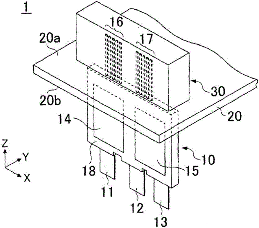
[0018] Figure 1A and Figure 1B is a diagram showing a semiconductor device according to a first embodiment of the present invention, in which, Figure 1A is the perspective view, and Figure 1B is parallel to Figure 1A A cross-sectional view taken in the YZ plane of , and through the plane of the male terminal 16 (described below). like Figure 1A and Figure 1B As shown, the semiconductor device 1 includes a semiconductor module 10 , a substrate 20 and a connector 30 . In this semiconductor device 1 , the male terminals 16 , 17 which are external connection terminals of the semiconductor module 10 are fitted to the female terminals 31 provided in the connector 30 through the substrate 20 .

[0019] Hereinafter, the semiconductor device 1 will be described. First, the semiconductor module 10, the substrate 20, and the connector 30 will be briefly described, and then, the structure of the portion where the male terminals 16, 17 of the semiconductor module 10 are fitted to...

no. 2 example

[0073] In the second embodiment, the hardness (Vickers hardness) of the metal film 163 as the surface treatment material of the male terminal 16 and the hardness of the metal film 312 as the surface treatment material of the female terminal 31 are made different from each other. Specifically, the hardness of the metal film 312 of the female terminal 31 is made higher than the hardness of the metal film 163 of the male terminal 16 . That is, the metal film 312 of the female terminal 31 is made harder than the metal film 163 of the male terminal 16 .

[0074] Image 6 It is a graph showing the relationship between the Vickers hardness and the amount of deformation of the metal film 312 of the female terminal 31 . In this case, the Vickers hardness of the metal film 163 of the male terminal 16 is fixed at 100 Hv. exist Image 6 In , gold films having the same thickness are used as the metal film 163 and the metal film 312. exist Image 6 , the contact pressure P is set to 4N...


PUM

PropertyMeasurementUnit
thicknessaaaaaaaaaa
thicknessaaaaaaaaaa
Vickers hardnessaaaaaaaaaa

Abstract

A terminal connecting structure includes: a male terminal (16); and a female terminal (31) to which the male terminal is fitted. The male terminal includes a first metal material (161) and a first metal film (163) that is formed on an outermost surface of the male terminal to coat the first metal material directly or indirectly. The female terminal includes a second metal material (311) and a second metal film (312) that is formed on an outermost surface of the female terminal to coat the second metal material directly or indirectly. A hardness of the first metal material is different from a hardness of the second metal material.

Description

technical field [0001] The present invention relates to a terminal connection structure and a semiconductor device including the terminal connection structure. Background technique [0002] There is known a structure in which an external connection terminal (convex side) of an electronic component is inserted into a through-hole (concave side) of a substrate and connected to a wiring of the substrate by soldering or the like. Examples of such a structure include a semiconductor device in which external connection terminals of a semiconductor module having a resin-sealed semiconductor element are inserted into through-holes of a substrate and connected to wiring of the substrate by soldering or the like (for example, refer to Japanese Patent Application Laid-Open No. 2010-199622 (JP 2010-199622 A)). [0003] However, in the above technique, since a process of connecting the terminal to the wiring by soldering or the like is necessary, the manufacturing process is complicated...

Claims


Application Information

Patent Timeline
Patent Type & Authority Applications(China)
IPC IPC(8): H01R13/03H01R12/71H01R13/05H01R13/11
CPCH01R12/716H01R13/03H01R13/05H01R13/11H01R2201/26
Inventor 门口卓矢平野敬洋原田新奥村知巳福谷啓太西畑雅由
Owner TOYOTA JIDOSHA KK