
In-cell touch liquid crystal panel and array substrate thereof

An array substrate and liquid crystal panel technology, applied in optics, instruments, electrical and digital data processing, etc., can solve the problems of inability to improve touch sensitivity and reduce the aperture ratio of the display area, and achieve the effects of improving touch sensitivity and reducing impedance

Active Publication Date: 2016-09-07
WUHAN CHINA STAR OPTOELECTRONICS TECH CO LTD
View PDF7 Cites 14 Cited by
  • Summary
  • Abstract
  • Description
  • Claims
  • Application Information

AI Technical Summary

Problems solved by technology

In the case that the length, thickness and resistivity of the third metal layer 6 remain unchanged, in order to reduce the impact of the trace impedance of the metal connection line 6a on the touch signal, if the width of a single metal connection line 6a is increased, then It will reduce the aperture ratio of the display area; if multiple metal connecting wires 6a are connected to one touch sensing electrode 5a in parallel, the total resistance of the wires will be reduced, but increasing the number of metal connecting wires 6a will increase the contact with the touch sensor. The coupling capacitance formed between the sensing electrodes 5a cannot improve the touch sensitivity

Method used


Image

  • In-cell touch liquid crystal panel and array substrate thereof
  • In-cell touch liquid crystal panel and array substrate thereof
  • In-cell touch liquid crystal panel and array substrate thereof

Examples


Embodiment Construction

[0027] In order to make the object, technical solution and advantages of the present invention clearer, the specific implementation manners of the present invention will be described in detail below in conjunction with the accompanying drawings. Examples of these preferred embodiments are illustrated in the accompanying drawings. The embodiments of the invention shown in and described with reference to the drawings are merely exemplary, and the invention is not limited to these embodiments.

[0028] Here, it should also be noted that, in order to avoid obscuring the present invention due to unnecessary details, only the structures and / or processing steps closely related to the solution according to the present invention are shown in the drawings, and the related Other details are not relevant to the invention.

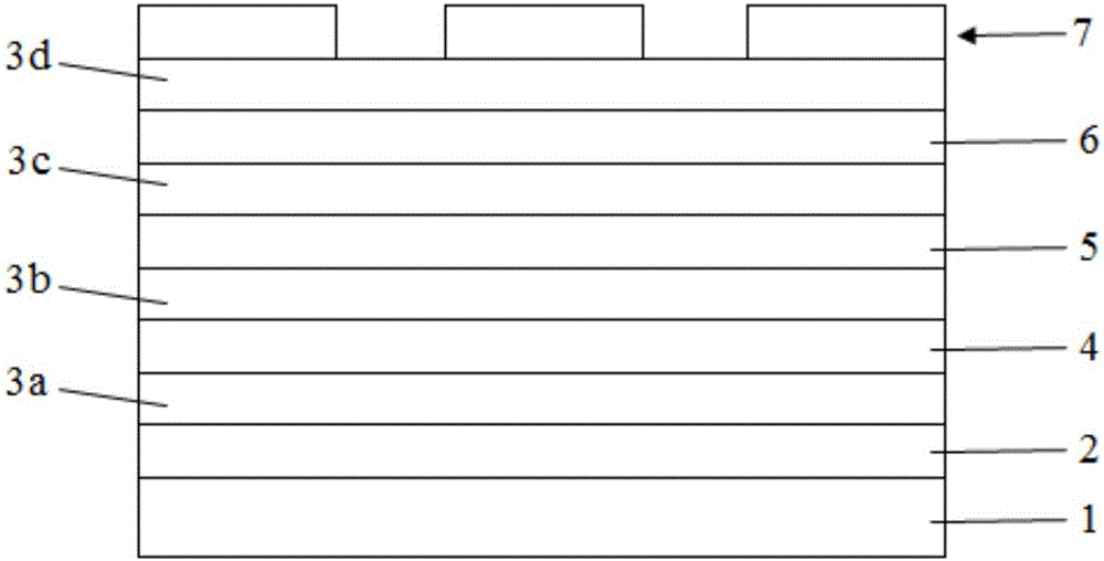
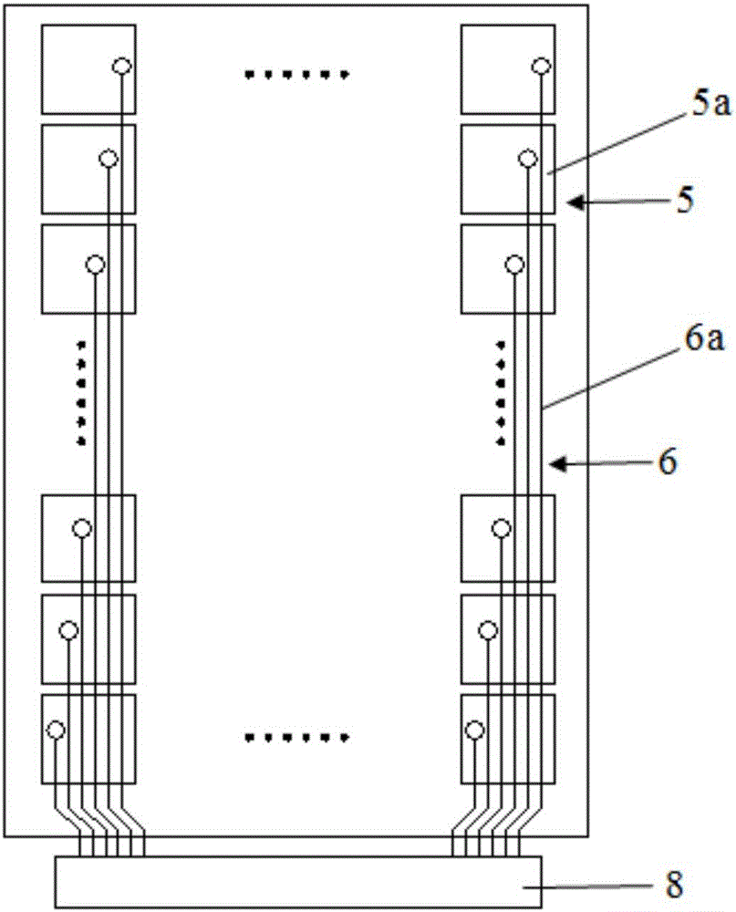
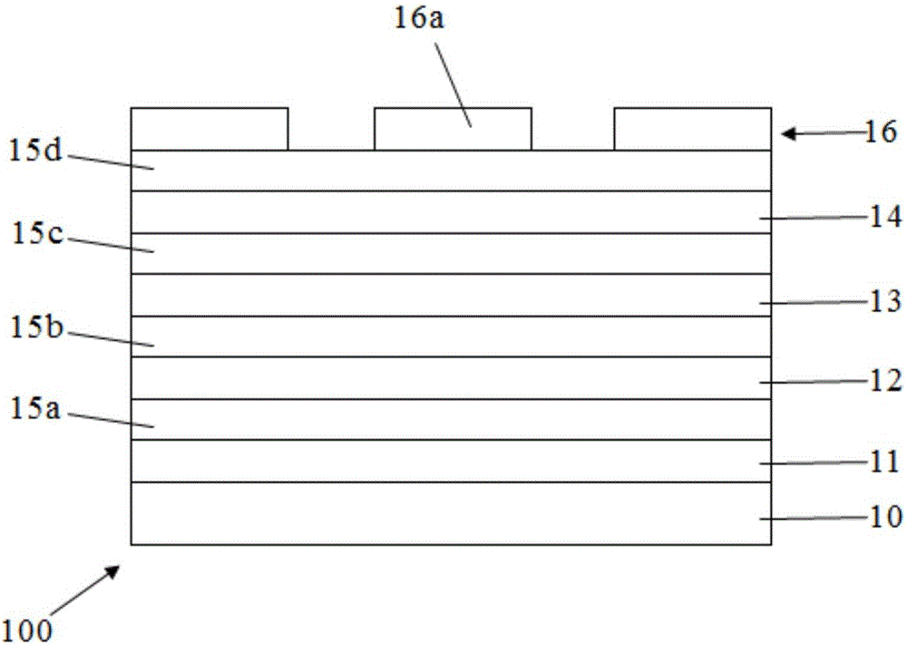
[0029] refer to Figure 3-Figure 8 , this embodiment first provides an array substrate embedded with a touch liquid crystal panel, and the touch structure is embedde...


PUM


Abstract

The invention discloses an in-cell touch liquid crystal panel and an array substrate thereof. The array substrate comprises a glass substrate, a first metal layer, a second metal layer, a third metal layer and a common electrode layer, wherein the first metal layer, the second metal layer, the third metal layer and the common electrode layer are formed on the glass substrate and are mutually insulated; a plurality of scanning lines are arranged in the second metal layer; a plurality of connection lines are arranged in the third metal layer; the common electrode layer is segmented into a plurality of touch induction electrodes, and the touch induction electrodes are electrically connected to a touch detection chip through the connection lines; and a plurality of metal lines are also arranged in the second metal layer, the metal lines and the scanning lines are mutually insulated, and two ends of each metal line are independently electrically connected to the connection line just above the metal line, wherein a second direction and a first direction are mutually vertical. The in-cell touch liquid crystal panel and the array substrate thereof can reduce the impendence of the connection lines of the touch induction electrodes and improve touch flexibility.

Description

technical field [0001] The invention relates to the field of touch technology, in particular to an embedded touch liquid crystal panel and an array substrate thereof. Background technique [0002] As an input medium, the touch display screen is currently the simplest and most convenient way of human-computer interaction, so the touch display screen is more and more applied to various electronic products. Based on different working principles and information transmission media, touch screen products can be divided into four types: infrared touch screen, capacitive touch screen, resistive touch screen and surface acoustic wave touch screen; among them, capacitive touch screen has long life, high light transmittance, and can support multiple Point touch and other advantages have become the current mainstream touch screen technology. Capacitive touch screens include surface capacitive and projected capacitive, and projected capacitive can be further divided into self-capacitive...

Claims


Application Information

Patent Timeline
IPC IPC(8): G06F3/041G06F3/044G02F1/1333
CPCG02F1/13338G06F3/0412G06F3/044G06F2203/04111G06F3/041G06F3/0445G06F3/0446G02F1/136286H01L27/124
Inventor 邹恭华王英琪黄俊宏
Owner WUHAN CHINA STAR OPTOELECTRONICS TECH CO LTD
Features
  • Generate Ideas
  • Intellectual Property
  • Life Sciences
  • Materials
  • Tech Scout
  • Unparalleled Data Quality
  • Higher Quality Content
  • 60% Fewer Hallucinations
Learn More