
Photosensitive device, display panel and display device

A technology of photosensitive devices and display panels, which is applied in the direction of semiconductor devices, electric solid devices, electrical components, etc., can solve the problems of unsatisfactory photosensitive effects and low sensitivity of photosensitive devices, achieve high recognition efficiency and speed, expand the scope of application, and improve The effect of sensitivity

Active Publication Date: 2016-09-28
BOE TECH GRP CO LTD +1
View PDF3 Cites 9 Cited by
  • Summary
  • Abstract
  • Description
  • Claims
  • Application Information

AI Technical Summary

Problems solved by technology

[0002] Existing photosensitive devices are generally made of diodes, and their photosensitive effects are not ideal
Moreover, the sensitivity of the photosensitive device made of the currently occurring amorphous silicon thin film transistor is not high. Therefore, it is urgent to find a photosensitive device used in the field of low temperature polysilicon thin film transistor.

Method used


Image

  • Photosensitive device, display panel and display device
  • Photosensitive device, display panel and display device
  • Photosensitive device, display panel and display device

Examples


Embodiment Construction

[0029] In order to make the purpose, technical solutions and advantages of the present invention clearer, the present invention will be further described in detail below in conjunction with the accompanying drawings. Obviously, the described embodiments are only some of the embodiments of the present invention, rather than all of them. Based on the embodiments of the present invention, all other embodiments obtained by persons of ordinary skill in the art without making creative efforts belong to the protection scope of the present invention.

[0030] The technical solution involved in the present invention will be described in detail through specific examples below, and the present invention includes but is not limited to the following examples.

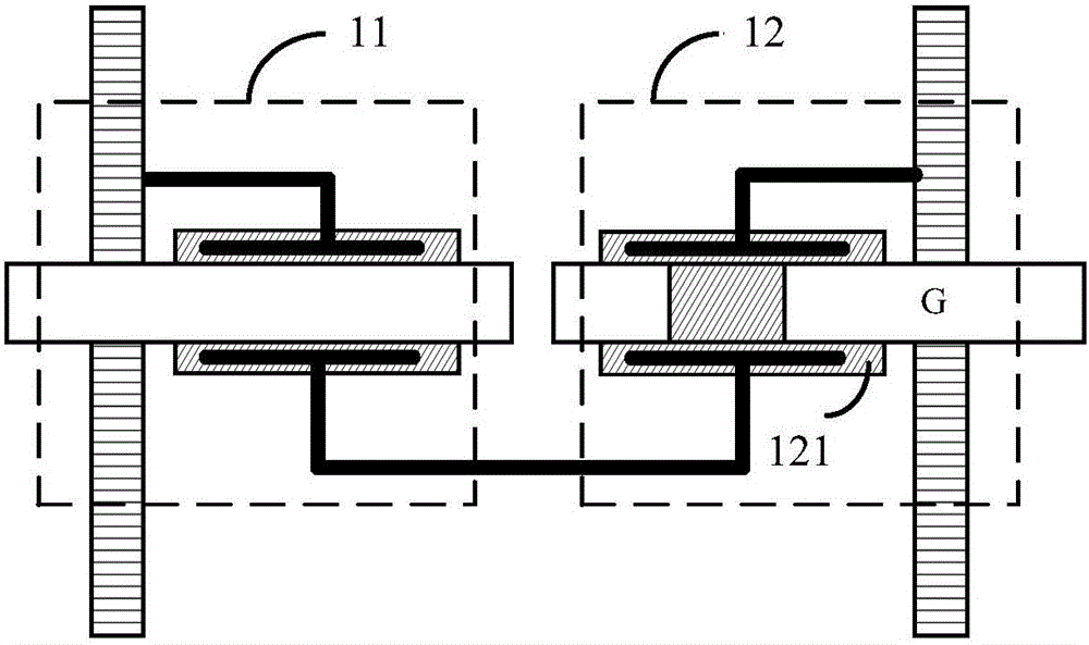
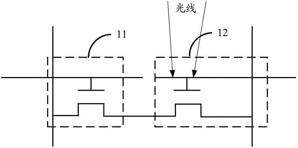
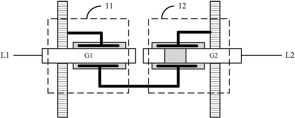
[0031] As shown in Figure 1(a), it is a schematic structural diagram of a photosensitive device provided by an embodiment of the present invention. The second thin film transistor 12 of the photosensitive unit; wherein, the first th...


PUM


Abstract

The invention relates to the technical field of semiconductors, and particularly relates to a photosensitive device and a photosensitive apparatus, aiming to realize the light intensity identification in a low-temperature polysilicon thin film transistor. The photosensitive device includes a top-gate type first thin film transistor used as a control switch and a top-gate type second thin film transistor connected with the first thin film transistor and used as a photosensitive unit, the grid of the second thin film transistor is at least partially transparent and is corresponding to part of the active layer in the second thin film transistor, so that the light intensity identification of the second thin film transistor can be realized when the two thin film transistors are conducted at the same time. In addition, the second thin film transistor can effectively distinguish the reading condition of the current signal at the output signal end under the different light irradiation, so that the sensitivity of the photosensitive device is improved. The photosensitive device realizes the light intensity induction in the top-gate type thin film transistors, the application of photosensitive devices is widen, and the identification efficiency and speed are relatively high.

Description

technical field [0001] The invention relates to the technical field of semiconductors, in particular to a photosensitive device, a display panel, and a display device. Background technique [0002] Existing photosensitive devices are generally made of diodes, and their photosensitive effects are not ideal. Moreover, the sensitivity of photosensitive devices made of amorphous silicon thin film transistors that appear at present is not high. Therefore, it is urgent to find a photosensitive device used in the field of low temperature polycrystalline silicon thin film transistors. Contents of the invention [0003] Embodiments of the present invention provide a photosensitive device and a photosensitive device, which are used to realize the purpose of identifying light intensity in a low-temperature polysilicon thin film transistor. [0004] Embodiments of the present invention adopt the following technical solutions: [0005] A photosensitive device, comprising: a first thi...

Claims


Application Information

Patent Timeline
IPC IPC(8): H01L27/14H01L27/15
CPCH01L27/14H01L27/15H01L31/115H01L27/14612H01L27/14659H01L31/02019H01L29/4908H01L29/78675H01L27/1251H01L31/03682H01L31/1136H01L31/119
Inventor 刘英明董学薛海林王海生陈小川丁小梁杨盛际许睿李昌峰刘伟王鹏鹏
Owner BOE TECH GRP CO LTD
Features
  • Generate Ideas
  • Intellectual Property
  • Life Sciences
  • Materials
  • Tech Scout
  • Unparalleled Data Quality
  • Higher Quality Content
  • 60% Fewer Hallucinations
Learn More