Organic electroluminescence diode substrate and preparation method and display apparatus thereof

A luminescent and diode technology, applied in the fields of organic electroluminescent diode substrates and their preparation methods, and display devices, can solve the problems of unfavorable light and thin display panels, low integration of substrates, and thick thickness, so as to improve integration and add value effect

Active Publication Date: 2016-09-28
BOE TECH GRP CO LTD
View PDF6 Cites 35 Cited by
  • Summary
  • Abstract
  • Description
  • Claims
  • Application Information

AI Technical Summary

Problems solved by technology

[0005] For OLED substrates with touch functions, it is usually necessary to prepare touch electrodes and sensing electrodes on the substrates on which OLED devices have been formed. However, the integration of such substrates is relatively low and the thickness is relatively thick, which is not conducive to thinner display panel

Method used


Image

  • Organic electroluminescence diode substrate and preparation method and display apparatus thereof
  • Organic electroluminescence diode substrate and preparation method and display apparatus thereof
  • Organic electroluminescence diode substrate and preparation method and display apparatus thereof

Examples


Embodiment 1

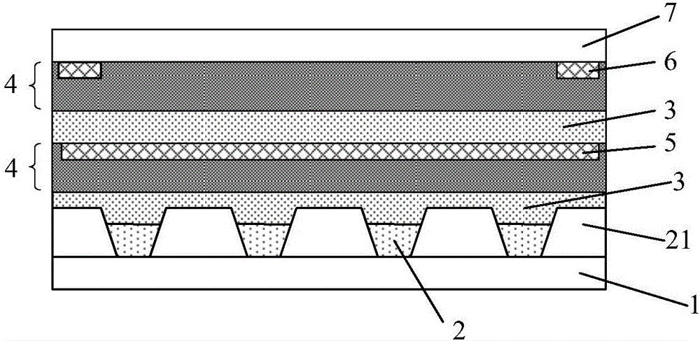
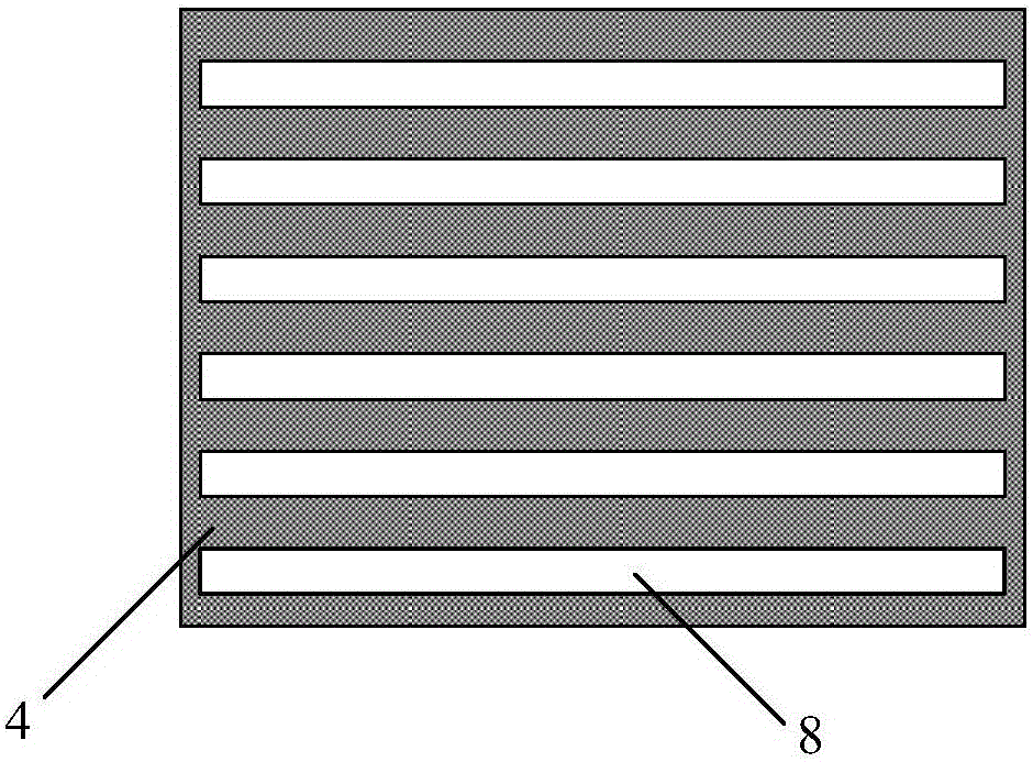
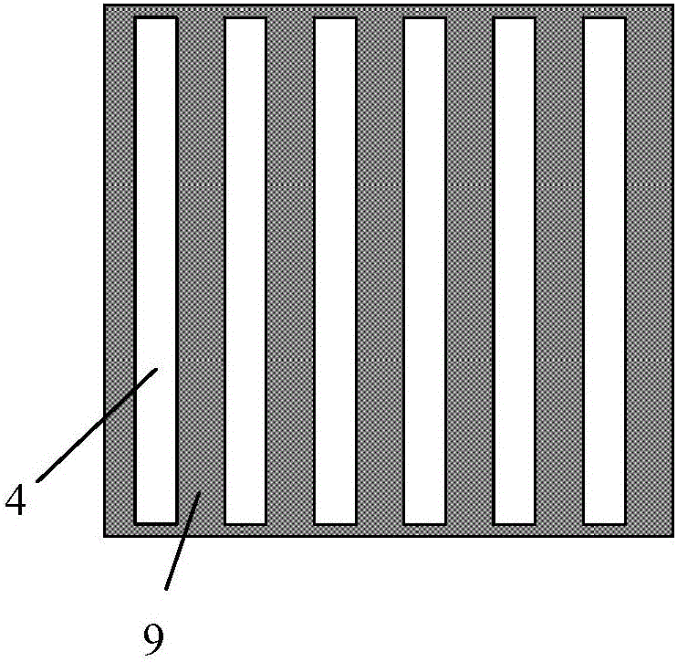
[0064] combine Figure 1-3 As shown, this embodiment provides an organic electroluminescent diode substrate, including a substrate 1, an organic electroluminescent unit 2 disposed on the substrate 1, and N groups of thin films disposed on the organic electroluminescent unit 2 N is an integer greater than or equal to 2, and each thin film group includes an inorganic film layer 3 and an organic film layer 4 arranged in sequence along a direction away from the organic electroluminescence unit 2 . Wherein, the inorganic film layer 3 is a barrier layer for preventing water, oxygen, etc. from polluting the organic electroluminescence unit 2, and the organic film layer 4 is a flat layer for providing a flat surface. In particular, any two layers in the multilayer organic film layer 4 of this embodiment are selected, and a plurality of first grooves 8 are arranged in one layer, and a plurality of second grooves 9 are arranged in the other layer, and a plurality of grooves 9 are arrang...

Embodiment 2

[0078] combine Figure 5-13 As shown, this embodiment provides a method for preparing an organic electroluminescent diode substrate, wherein the organic electroluminescent diode substrate can be the organic electroluminescent diode substrate in embodiment 1. In this embodiment, taking N=2 as an example, the preparation method in this embodiment is described, and the method specifically includes the following steps:

[0079] Step 1. On the substrate 1, an organic electroluminescent unit 2 is formed (taking a top emission type organic electroluminescent unit as an example for description), as Figure 6 shown.

[0080] Specifically, step 1 may include: 1) using a sputtered anode conductive film on the substrate 1, and forming a pattern including an anode layer through a patterning process; 2) forming a pattern including The pattern of the pixel definition layer 21; 3) On the substrate 1 formed with the pixel definition layer 21, a vacuum evaporation process is used to form a li...

Embodiment 3

[0093] This embodiment provides a display device, which includes the organic electroluminescent diode substrate described in Embodiment 1, so the display device of this embodiment has high integration and high added value, and can be applied to flexible displays.

[0094] The display device can be any product or component with a display function such as electronic paper, OLED panel, mobile phone, tablet computer, television, monitor, notebook computer, digital photo frame, navigator, etc.


PUM


Abstract

The invention provides an organic electroluminescence diode substrate and a preparation method and a display apparatus thereof, and belongs to the field of display technology. The organic electroluminescence diode substrate includes a substrate, an organic electroluminescence unit arranged on the substrate, and N groups of film sets which are arranged on the organic electroluminescence unit. N is an integer which is equal to or greater than 2. Each group of film set includes an inorganic film layer and an organic film layer which are successively arranged away from the direction of the organic electroluminescence unit, and one layer of the organic film layers is provided with a plurality of first grooves, and the other layer of the organic film layers is provided with a plurality of second grooves. The plurality of first grooves and the plurality of second grooves are intersected in orthographic projection on the substrate. Each first groove is filled with a first lead. Each second groove is filled with a second lead. According to the invention, the organic electroluminescence diode substrate is suitable for flexible display panels.

Description

technical field [0001] The invention belongs to the field of display technology, and in particular relates to an organic electroluminescence diode substrate, a preparation method thereof, and a display device. Background technique [0002] In the field of optoelectronic display technology, Organic Light Emitting Diode (OLED) has many advantages such as active light emission, high brightness, high contrast, ultra-thin, low power consumption, large viewing angle and wide operating temperature range. An advanced new flat panel display device with a wide range of applications. [0003] However, due to the inherent characteristics of organic materials, it is easy to absorb water and oxygen, and it is easy to wear and deteriorate after being eroded by water and oxygen, which greatly affects the life of the device. Therefore, OLED devices have high requirements for packaging. [0004] At present, the encapsulation technology of OLED devices is becoming more and more mature, includ...

Claims


Application Information

Patent Timeline
Patent Type & Authority Applications(China)
IPC IPC(8): H01L27/32H01L21/77H01L51/52H01L51/56
CPCH01L21/77H10K59/123H10K59/125H10K59/131H10K50/30H10K71/00G06F3/0412G06F2203/04103G06F3/0446G06F3/0445H10K59/40H10K50/8445H10K50/80H10K59/00H10K59/122H10K59/124H10K59/179H10K59/1275
Inventor 黄维
Owner BOE TECH GRP CO LTD
Why Eureka
Try Eureka