

an ultraviolet light emitting diode
A technology of light-emitting diodes and light-emitting areas, which is applied in semiconductor devices, electrical components, circuits, etc., to achieve the effect of improving light-extraction efficiency and improving external quantum efficiency.
- Summary
- Abstract
- Description
- Claims
- Application Information
AI Technical Summary
Problems solved by technology
Method used
Image


Examples
Embodiment 1
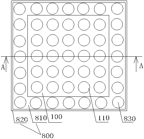
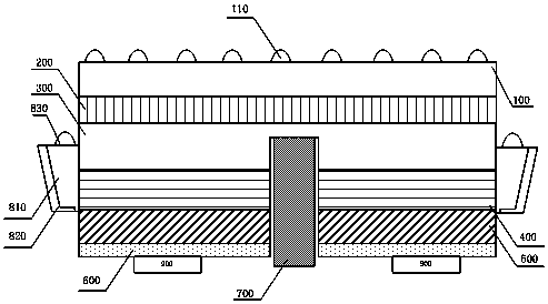
[0031] Such as Figure 1-Figure 2 As shown, the ultraviolet light emitting diode of this embodiment includes a substrate 100 , a buffer layer 200 , an N-type semiconductor layer 300 , a light-emitting region 400 , a P-type semiconductor layer 500 and a contact layer 600 which are sequentially formed. The ultraviolet light emitting diode further includes a P-type electrode 900 and an N-type electrode 700 , the P-type electrode 900 is distributed on the contact layer 600 , and the N-type electrode 700 is in contact with the N-type semiconductor layer 300 . A first light reflector 800 for guiding the light emitted from the side of the light emitting region 400 to the light emitted from the front is arranged on the side of the light emitting region 400 . The first light reflector 800 can guide the light emitted from the light-emitting area 400 to the side to the forward light-emitting surface of the ultraviolet light-emitting diode, and the light is emitted from the forward light-...
Embodiment 2
[0040] Such as Figure 3-5 As shown, based on the first embodiment above, this embodiment further improves the arrangement of the P-type electrode 500 and the N-type electrode 300 of the ultraviolet light-emitting diode. The N-type electrode 300 is no longer located at a corner of the ultraviolet light-emitting diode, but the P The type electrode 500 is disposed on the periphery of the N-type electrode 300 to improve the uniformity of the current between the P-type electrode 500 and the N-type electrode 300 and improve the luminous efficiency.
[0041] Specifically, such as Figure 4 As shown, in this embodiment, the N-type semiconductor layer 300 is provided with a groove 310 , and the light-emitting region 400 , the P-type semiconductor layer 500 and the contact layer 600 are all provided with through holes 410 , 510 , 610 connected in sequence. The through hole 410 of the light emitting region 400 communicates with the groove 310 , the groove 310 and the through holes 410 ...
Embodiment 3
[0048] Such as Figure 6 As shown, this embodiment is further improved on the basis of the second embodiment, and there is an insulating layer 710 isolating the N-type electrode 700 from the light emitting region 400 , the P-type semiconductor layer 500 and the contact layer 600 in the through holes 410 , 510 , 610 .
[0049] Among them, the insulating layer is Al 2 o 3 or SiO 2 The material can effectively prevent the contact between the N-type electrode 700 and the light emitting region 400 , the P-type semiconductor layer 500 and the contact layer 600 , and avoid short circuit.
PUM
 Abstract
Description
Claims
Application Information