Multilayer printed circuit board drilling method

A printed circuit board, multi-layer printing technology, applied in the direction of printed circuit, printed circuit manufacturing, electrical components, etc., can solve the problems of destroying signal integrity, low efficiency, high price of blind hole or buried hole process, and avoid process price High, reduce length, avoid the effect of inefficiency

Active Publication Date: 2016-09-28
WUHAN CHINA STAR OPTOELECTRONICS TECH CO LTD
View PDF5 Cites 4 Cited by
  • Summary
  • Abstract
  • Description
  • Claims
  • Application Information

AI Technical Summary

Problems solved by technology

[0002] The stacked structure of the existing multilayer printed circuit board such as figure 1 As shown, the metal layers are connected by vias. However, a section of these vias that is not used for signal transmission and useless hole wall copper will increase the loss of signal transmission in the printed circuit board, and even destroy the integrity of the signal. Therefore, blind or buried vias are commonly used in the industry to replace these vias (such as figure 2 shown), but the process of blind or buried vias is expensive and inefficient

Method used


Image

  • Multilayer printed circuit board drilling method
  • Multilayer printed circuit board drilling method
  • Multilayer printed circuit board drilling method

Examples


Embodiment Construction

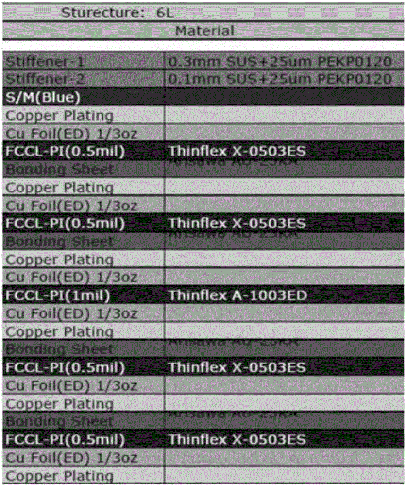
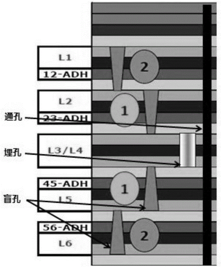
[0033] see image 3 and Figure 4 , is the flow chart and process flow chart of the first embodiment of the multilayer printed circuit board drilling method of the present invention. In this embodiment, the multilayer printed circuit board is a flexible printed circuit board, and the flexible printed circuit board is a high Reliable and flexible printed circuit, referred to as soft board, has the characteristics of high wiring density, light weight, and thin thickness. It is mainly used in mobile phones, notebook computers, PDAs, digital cameras, LCM and other products. And in this embodiment, the flexible printed circuit board is a 4-layer printed circuit board, which includes first to fourth metal layers 11 - 14 and an insulating layer 15 spaced between every two metal layers.

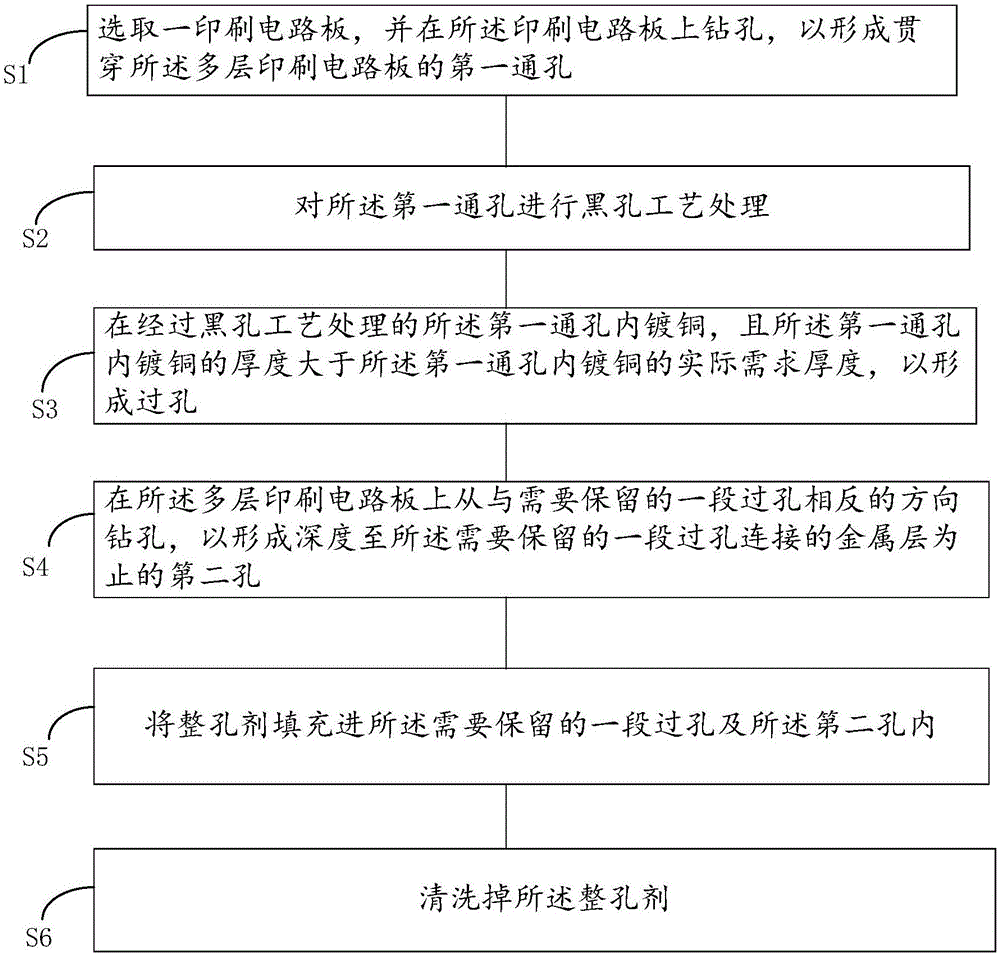
[0034] The multilayer printed circuit board drilling method includes:

[0035] Step S1: Select a printed circuit board, and drill holes on the printed circuit board to form a first through hole pe...


PUM


Abstract

The invention discloses a multilayer printed circuit board drilling method. The method comprises the steps that a printed circuit board is selected, and a hole is drilled on the printed circuit board so that a first through hole penetrating through the multilayer printed circuit board is formed; black hole technology processing is performed on the first through hole; copper is plated in the first through hole through black hole technology processing, and the thickness of the plated copper in the first through hole is greater than the actually required thickness of the plated copper in the first through hole so that a via hole is formed; drilling is performed on the multilayer printed circuit board from a direction opposite to a segment of via hole required to be reserved so that a second hole of which the depth extends to a metal layer connected with the segment of via hole required to be reserved is formed; a hole filling agent is filled in the segment of via hole required to be reserved and the second hole; and the hole filling agent is washed so that the length of useless hole copper can be reduced, integrity of signal transmission can be guaranteed, and the problems of high process price and low efficiency caused by arrangement of blind holes and buried holes on the printed circuit board can be avoided.

Description

technical field [0001] The invention relates to the technical field of printed circuit boards, in particular to a drilling method for multilayer printed circuit boards. Background technique [0002] The stacked structure of the existing multilayer printed circuit board such as figure 1 As shown, the metal layers are connected by vias. However, a section of these vias that is not used for signal transmission and useless hole wall copper will increase the loss of signal transmission in the printed circuit board, and even destroy the integrity of the signal. Therefore, blind or buried vias are commonly used in the industry to replace these vias (such as figure 2 shown), but the process of blind or buried vias is expensive and inefficient. Contents of the invention [0003] The technical problem mainly solved by the present invention is to provide a low-cost and high-efficiency multilayer printed circuit board drilling method to reduce the length of copper in useless holes ...

Claims


Application Information

Patent Timeline
Patent Type & Authority Applications(China)
IPC IPC(8): H05K3/00
CPCH05K3/0047H05K2203/0214
Inventor 陈娟
Owner WUHAN CHINA STAR OPTOELECTRONICS TECH CO LTD
Why Eureka
Try Eureka