A FPGA implementation system and method for oversampling data clock recovery

A technology of data clock and implementation method, which is applied in the direction of data error detection, electrical digital data processing, response error generation, etc. with redundancy in operation, can solve problems such as insufficient GE port dedicated pins, and achieve reduced cost effect

Active Publication Date: 2019-03-29
OPHYLINK COMM TECH
View PDF2 Cites 0 Cited by
  • Summary
  • Abstract
  • Description
  • Claims
  • Application Information

AI Technical Summary

Problems solved by technology

[0004] The purpose of the present invention is to provide an FPGA implementation system and method for oversampling data clock recovery, aiming at the problem that sufficient GE port dedicated pins cannot be provided on the FPGA chip, a method that can also realize data clock recovery through ordinary IO is designed ;Using ordinary IO for data recovery can flexibly meet various needs, and the number of implementations is no longer limited to the dedicated pins that come with the chip

Method used


Image

  • A FPGA implementation system and method for oversampling data clock recovery
  • A FPGA implementation system and method for oversampling data clock recovery
  • A FPGA implementation system and method for oversampling data clock recovery

Examples


Embodiment 1

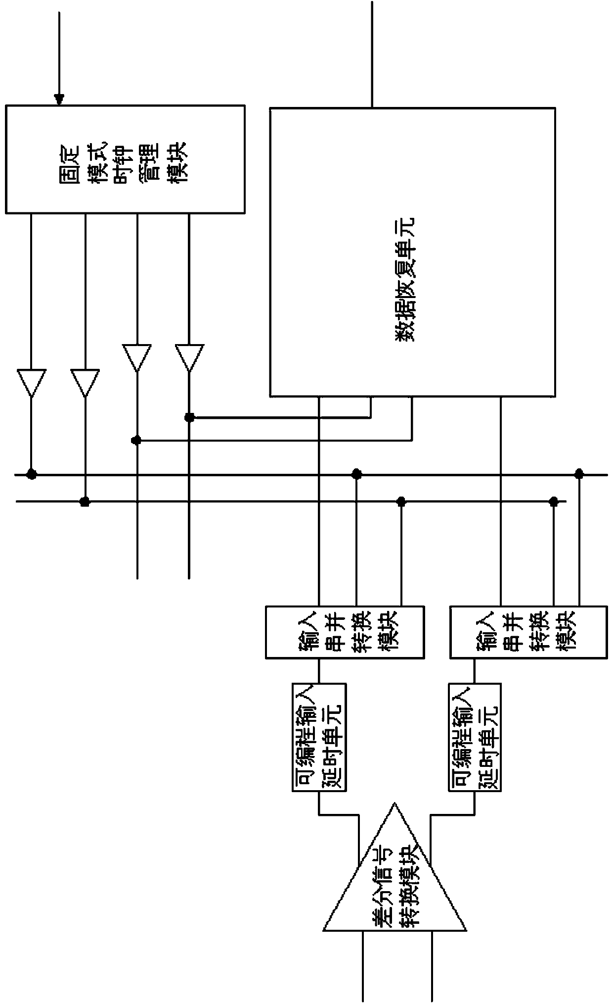
[0042] An FPGA implementation system for oversampling data clock recovery, such as figure 1 As shown, it includes a differential signal conversion module, a programmable input delay unit, an input serial-to-parallel conversion module and a fixed-mode clock management module arranged in the FPGA, the differential signal conversion module is connected to a programmable input delay unit, and the The programmable input delay unit is connected to the input serial-to-parallel conversion module, and the input serial-to-parallel conversion module is connected to the fixed-mode clock management module.

[0043] The differential signal conversion module is used to buffer the input differential signal sent into the FPGA from the outside and divide it into two differential signals inside the FPGA;

[0044] The programmable input delay unit delays the differential signal inside the FPGA;

[0045]The input serial-to-parallel conversion module samples the signal output in the programmable i...

Embodiment 2

[0048] This embodiment is further optimized on the basis of the above embodiments, such as figure 1 As shown, further in order to better realize the system of the present invention, the data collected in the input serial-to-parallel conversion module can be recovered, and the following setting method is particularly adopted: a data recovery unit is also included, and the data recovery unit It is connected to the input serial-to-parallel conversion module, and the fixed-mode clock management module is also connected to the data recovery unit.

Embodiment 3

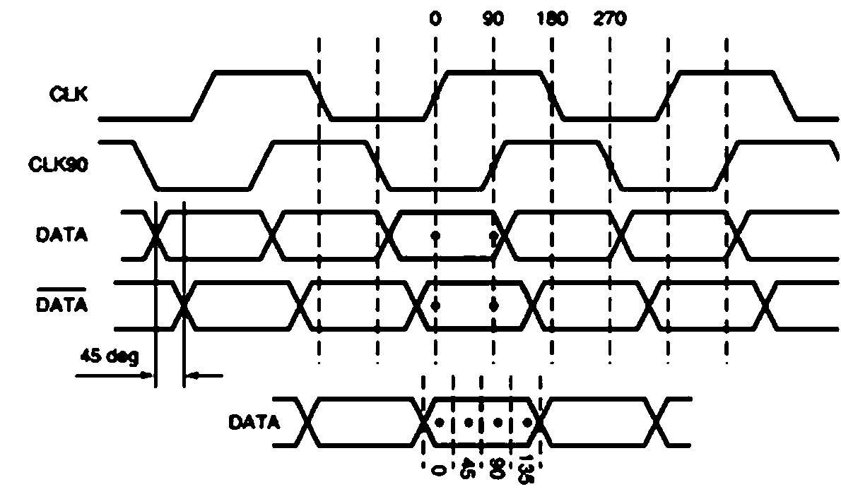
[0050] This embodiment is further optimized on the basis of the above embodiments, such as figure 1 As shown, further in order to better realize the system of the present invention, the following setting method is adopted in particular: the programmable input delay unit is two and the output signal between the two programmable input delay units exists 45 ° phase difference, the two programmable input delay units are connected to the differential signal conversion module and the input serial-to-parallel conversion module.


PUM


Abstract

The invention discloses an oversampling data clock recovery FPGA realizing system and method; the system comprises a differential signal conversion module arranged in the FPGA, a programmable input delay unit, an input serial-parallel conversion module and a fixed mode clock management module; the differential signal conversion module is connected with the programmable input delay unit; the programmable input delay unit is connected with the input serial-parallel conversion module; the input serial-parallel conversion module is connected with the fixedly mode clock management module. The differential signal conversion module carries out caching treatment for an external input differential signal sent into the FPGA, thus forming two FPGA internal differential signals; aiming at the problems that the FPGA chip cannot provide sufficient GE port special pins, the novel method can use a normal IO to realize data clock recovery; the method uses normal IO to carry out data recovery, thus flexibly satisfying various demands, and the realizing number can no longer be limited by special pins carried by the FPGA chip.

Description

technical field [0001] The invention relates to the relevant technical field of serial data recovery of a GE port in an FPGA chip on a communication device, and specifically relates to an FPGA implementation system and method for oversampling data clock recovery. Background technique [0002] At present, the data recovery of the GE interface on the FPGA chip firstly needs to send a reference clock to the processing module, and then use the reference clock to combine with the received serial data to recover the clock of the data sent by the peer end, and then upload the recovered clock to the After the global clock network, collect data and perform serial-to-parallel conversion. [0003] This function is put into the FPGA chip through the hard core IP, and correspondingly has dedicated pins. The number of dedicated pins supported by different chip models is also different. When the number of interfaces is required to be large, some high-end chips should be selected. Because ...

Claims


Application Information

Patent Timeline
Patent Type & Authority Patents(China)
IPC IPC(8): G06F11/14
CPCG06F11/1446
Inventor 邱建刚
Owner OPHYLINK COMM TECH
Why Eureka
Try Eureka