Array substrate, display panel and display device
An array substrate and seed pixel technology, which is applied in the fields of display panels, display equipment and array substrates, can solve the problems of increasing the display power consumption of the array substrate, and achieve the effect of reducing power consumption.
- Summary
- Abstract
- Description
- Claims
- Application Information
AI Technical Summary
Problems solved by technology
Method used
Image


Examples
Embodiment 1
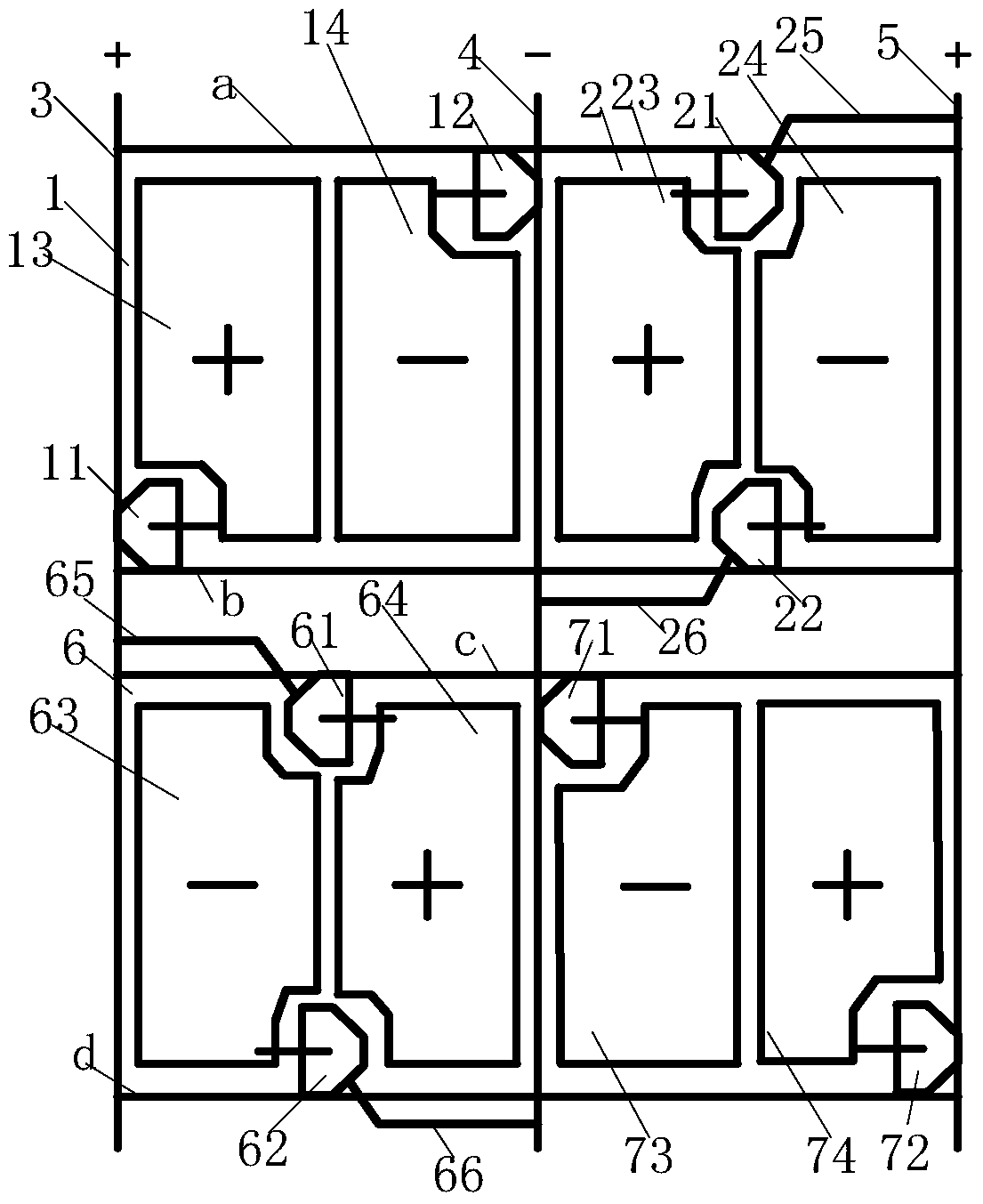
[0033] see figure 1 , an embodiment of the present invention provides an array substrate, the first row of the array substrate includes alternately arranged first pixel structures 1 and second pixel structures 2, the first pixel structures 1 are located on the first data line 3 and the second data line Between the lines 4, the second pixel structure 2 is located between the second data line 4 and the third data line 5, wherein the first row is any row in the array substrate.
[0034] The first pixel structure 1 includes two first sub-pixel electrodes arranged side by side, the first sub-pixel electrode is close to its corresponding target data line, the polarity of the first sub-pixel electrode and its corresponding target data line are the same, and the first sub-pixel electrode The TFT corresponding to the electrode is located on the side of the first sub-pixel electrode close to the target data line, and electrically connects the first sub-pixel electrode to the target data...
Embodiment 2
[0066] An embodiment of the present invention provides a display panel, including any array substrate provided in Embodiment 1.
Embodiment 3
[0068] An embodiment of the present invention provides a display device, including any display panel provided in Embodiment 2.
[0069] The serial numbers of the above embodiments of the present invention are for description only, and do not represent the advantages and disadvantages of the embodiments.
PUM
 Abstract
Description
Claims
Application Information