A kind of production method of p-channel vdmos device

A production method and device technology, applied in the fields of semiconductor devices, semiconductor/solid-state device manufacturing, electrical components, etc., can solve the problems of positive oxide charge accumulation, large Vth, impurity accumulation, etc., to reduce positive charges and avoid negative Impact, performance improvement effect

Active Publication Date: 2019-10-18
HUAYUE MICROELECTRONICS
View PDF3 Cites 0 Cited by
  • Summary
  • Abstract
  • Description
  • Claims
  • Application Information

AI Technical Summary

Problems solved by technology

[0004] A: The high-temperature heat treatment process causes heavily doped phosphorus impurities in polysilicon to easily cross the gate oxide and reach the channel surface, resulting in the accumulation of similar impurities, which directly leads to a larger Vth;
[0005] B: The influence of oxide charge, especially the high temperature process after the gate oxide will lead to positive oxide charge accumulation, and positive oxidation charge will cause the Vth of P-channel VDMOS to increase;

Method used


Image

  • A kind of production method of p-channel vdmos device
  • A kind of production method of p-channel vdmos device
  • A kind of production method of p-channel vdmos device

Examples


Embodiment Construction

[0028] A kind of P channel VDMOS device production method, comprises the steps:

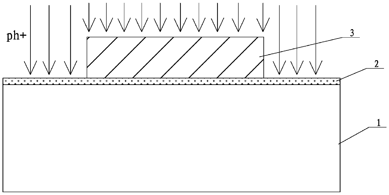
[0029] Step 1), after the active area of ​​the epitaxial layer 1 is opened, thin oxygen growth is performed first to form the oxide layer 2, and then the photoresist layer 3 is covered on the oxide layer 2, and the glue is partially removed according to the design requirements, and then the polycrystalline gate is used The photolithography plate is injected with N-type impurities (ph+) with glue, such as figure 1 shown;

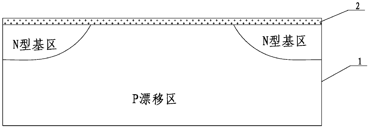
[0030] Step 2), remove the remaining photoresist on the oxide layer 2, and form the required N-type base junction depth on the upper surface of the epitaxial layer 1 after high-temperature annealing, such as figure 2 shown;

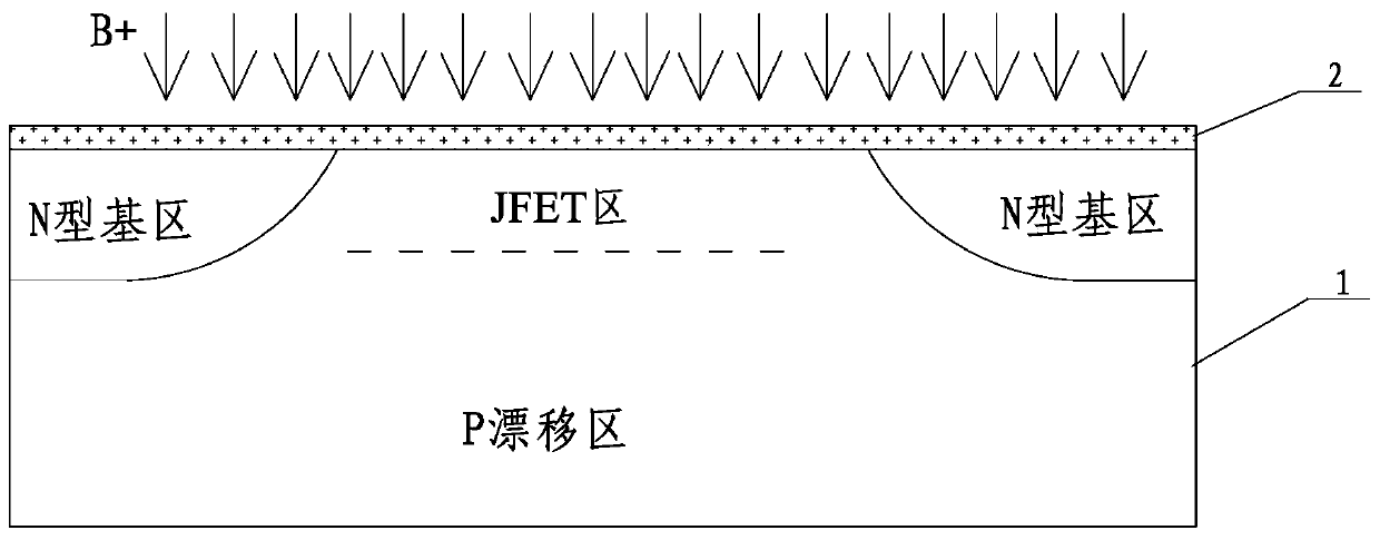
[0031] Step 3), perform comprehensive low-dose implantation of boron impurities (B+) on the oxide layer 2, and form a JFET region between the junction depths of the N-type base region, such as image 3 As shown, the comprehensive low-dose implantation o...


PUM


Abstract

The invention discloses a production method of a P-channel VDMOS device, which includes forming an oxide layer on the epitaxial layer, covering the oxide layer with a photoresist layer, and then injecting N-type impurities with glue; The required N-type base junction depth step; the boron impurity implantation step on the oxide layer; the gate oxide layer is formed on the epitaxial layer, and then polysilicon deposition and doping are performed on the gate oxide layer, and the polysilicon gate is used again Step of forming a polysilicon gate layer with a photolithography plate; covering a local area of ​​the gate oxide layer with photoresist, then directly performing source P+ processing, and forming a P+ region in the N-type base region; and finally depositing an inner metal insulating layer, and at the same time The upper surface and the lower surface of the epitaxial layer are respectively provided with a metal layer to form a standard VDMOS device step. The production method of the above-mentioned P-channel VDMOS device can stabilize the Vth value of the P-channel VDMOS device between 2 and 4V, which has extremely high stability and rationality.

Description

technical field [0001] The invention relates to a production method of a P-channel VDMOS device, which belongs to the field of semiconductor production. Background technique [0002] At present, the production process of P-channel VDMOS devices is basically the same as that of N-channel VDMOS devices, as follows: [0003] In the VTH formation process of N-type VDMOS devices, after the gate oxide growth and polysilicon gate etching are completed, a certain dose of P-type impurities is first implanted through the polysilicon gate self-alignment process, and then annealed at high temperature to form a P-type with a certain junction depth. The base region, and then use the polycrystalline gate self-alignment process to perform source N+ high-dose implantation and annealing. In this way, the channel is formed by the difference in the second lateral diffusion junction depth between the P-type base region and the N+ source region, and finally VTH The size is determined by the gate...

Claims


Application Information

Patent Timeline
Patent Type & Authority Patents(China)
IPC IPC(8): H01L29/78H01L21/336
Inventor 鄢细根何火军杨振赵铝虎潘国刚
Owner HUAYUE MICROELECTRONICS
Why Eureka
Try Eureka