Carrier implementation method for low common-mode voltage modulation of three-phase five-level inverter

A common-mode voltage and inverter technology is applied in the field of carrier realization of a three-phase five-level inverter low common-mode voltage modulation strategy, and can solve problems such as low total harmonic distortion rate

Active Publication Date: 2016-11-09
HEFEI UNIV OF TECH
View PDF6 Cites 23 Cited by
  • Summary
  • Abstract
  • Description
  • Claims
  • Application Information

AI Technical Summary

Problems solved by technology

[0012] In order to solve the problems of the common mode voltage of the five-level inverter, the balance of the flying capacitor voltage and the total harmonic distortion rate of the output phase current, the present invention proposes a method for realizing the carrier wave of the low common mode voltage modulation strategy, which can be achieved through the carrier wave The stacked modulation method enables the inverter to reduce the amplitude of the common-mode voltage to 1 / 12 of the total DC bus voltage in the entire linear working area, realize the balanced control of the flying capacitor, and ensure the total harmonics in the output phase current Low distortion rate, simple method and easy engineering application

Method used


Image

  • Carrier implementation method for low common-mode voltage modulation of three-phase five-level inverter
  • Carrier implementation method for low common-mode voltage modulation of three-phase five-level inverter
  • Carrier implementation method for low common-mode voltage modulation of three-phase five-level inverter

Examples


Embodiment Construction

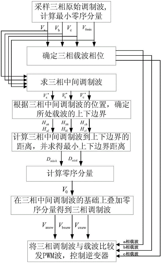
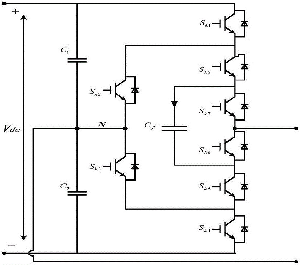
[0075] The circuit topology of each phase of the three-phase five-level inverter involved in the present invention is the same, and its single-phase topology diagram is as follows figure 2 shown. The total DC bus voltage is V dc , the DC side is provided with two capacitors C connected in series 1 and capacitance C 2 , capacitance C 1 The positive pole is connected to the positive pole of the inverter input, and the capacitor C 1 Negative electrode and capacitor C 2 The positive connection point is defined as the midpoint of the inverter; it contains 8 switching tubes, namely the switching tube S ki , i=1,2,3...8,k=a,b,c, where k represents the three-phase circuit of the inverter, that is, phase a, phase b, phase c; switch tube S k1 , switch tube S k5 , switch tube S k7 , switch tube S k8 , switch tube S k6 , switch tube S k4 in series, the switching tube S k1 The emitter is connected to the switch tube S k5 collector, switching tube S k5 The emitter is connecte...


PUM


Abstract

The invention discloses a carrier implementation method for low common-mode voltage modulation of a three-phase five-level inverter. The carrier implementation method comprises the steps of sampling a three-phase original modulation wave, and calculating a minimum zero-sequence component; determining the carrier phase according to the three-phase original modulation wave and the minimum zero-sequence component; superposing the minimum zero-sequence component on the three-phase original modulation wave so as to acquire a three-phase intermediate modulation wave; determining an upper boundary and a lower boundary of a located carrier according to the position of the three-phase intermediate modulation wave; calculating the distance between the three-phase intermediate modulation wave and the upper boundary and the distance between the three-phase intermediate modulation wave and the lower boundary, and solving the minimum distance between the upper boundary and the lower boundary; solving a zero-sequence component by using the acquired minimum distance; superposing the zero-sequence component on the three-phase intermediate modulation wave so as to acquire a corrected three-phase modulation wave; and finally comparing the corrected three-phase modulation wave with a three-phase carrier, and generating a PWM wave control five-level inverter. The carrier implementation method disclosed by the invention can realize the advantages of low common-mode voltage, small flying capacitive voltage fluctuation, low harmonic distortion and the like. Because of adoption of carrier implementation, the method is simple to implement, convenient to control and easy to be popularized to actual engineering.

Description

technical field [0001] The invention relates to the field of photovoltaic technology, in particular to a method for realizing a carrier wave of a three-phase five-level inverter low common-mode voltage modulation strategy. Background technique [0002] As a renewable energy source, solar energy has the advantages of being widely distributed, sustainable, and non-polluting. Photovoltaic power generation technology is one of the basic ways to effectively utilize solar energy resources. At present, various photovoltaic power generation technologies, including photovoltaic grid-connected, have received strong support from governments of various countries. [0003] In the photovoltaic power generation system, the five-level inverter has lower switching loss and current ripple than the commonly used three-level inverter. In the case of the same filter components, it has a lower current harmonic distortion rate. [0004] Same as the three-level inverter, the five-level inverter ...

Claims


Application Information

Patent Timeline
Patent Type & Authority Applications(China)
IPC IPC(8): H02M7/5395H02M1/44
CPCH02M1/44H02M7/5395
Inventor 王付胜李祯付航郑德佑张兴
Owner HEFEI UNIV OF TECH
Why Eureka
Try Eureka