Touch panel and manufacturing method thereof

A touch panel and manufacturing method technology, applied in the direction of instruments, electrical digital data processing, data processing input/output process, etc., can solve problems such as black matrix printing step difference, bubble defects, etc., to avoid height step difference, increase production capacity, Improve the effect of touch performance

Active Publication Date: 2016-11-16
INTERFACE OPTOELECTRONICS SHENZHEN +1
View PDF3 Cites 18 Cited by
  • Summary
  • Abstract
  • Description
  • Claims
  • Application Information

AI Technical Summary

Problems solved by technology

[0007] In view of this, the present invention aims at the deficiencies in the prior art, and its main purpose is to provide a touch panel and its ma

Method used


Image

  • Touch panel and manufacturing method thereof
  • Touch panel and manufacturing method thereof
  • Touch panel and manufacturing method thereof

Examples


Embodiment Construction

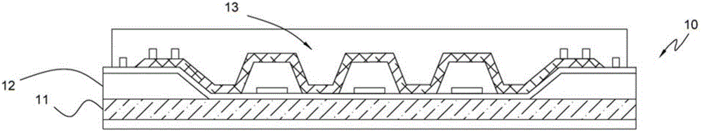
[0049] The invention discloses a touch panel and a manufacturing method thereof. The touch panel is applied to display devices, tablet computers, smart phones, notebook computers, desktop computers, televisions, satellite navigation, car displays, and aviation displays. or portable DVD players and other electronic devices, and touch screens can be divided into resistive touch screens and capacitive touch screens, of which capacitive touch panels mainly include film-type (Film-type ) and glass-type (Glass-type) touch panels, and the present invention mainly focuses on film-type touch panels, more particularly the structure of double-layer film-type (Glass-Flim-Flim, GFF) touch panels.

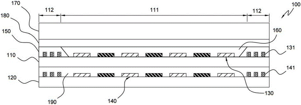
[0050] Please refer to image 3, is a cross-sectional structure diagram of the touch panel 100 provided by the embodiment of the present invention.

[0051] The touch panel 100 has a first substrate 110 and a second substrate 120 . Wherein, a sensing area 111 and a frame area 112 surrounding t...


PUM

PropertyMeasurementUnit
Thicknessaaaaaaaaaa

Abstract

The invention discloses a touch panel and a manufacturing method thereof. Different from a method of printing a black matrix on a cover glass by monolithic printing and then abutting the cover glass with a touch sensing structure, a method of using a yellow light lithography process is provided to replace the method, a black matrix photoresist is used to directly make a shading layer on the touch sensing structure, to cover a conductive circuit of a frame region. Then concave positions of the shading layer, exposed out of a sensing region are filled by a filling layer, and height of the filling layer is flushed with height of the shading layer. The touch panel can prevent fitting bubbles generated by printing segment difference, defects on appearance of the panel are reduced. Since the yellow light lithography process can make thickness of the shading layer reduce, touch efficacy is improved. the touch panel can be matched with multi-layout design, and capacity is greatly improved.

Description

technical field [0001] The present invention relates to a touch panel and its manufacturing method, in particular to a touch panel capable of improving black matrix printing level difference and its manufacturing method. Background technique [0002] Thanks to the progress of science and technology, portable electronic devices can be seen everywhere in people's lives, such as notebook computers, tablet computers, smart phones, etc., and with the increasing dependence of users, the functions of portable electronic devices are also increasing. Thereupon, it becomes more and more powerful; the common feature of such products is that they have a display screen, which can display various multimedia audio and video to users. Furthermore, in recent years, the trend of portable electronic devices is to provide touch operations with larger screens to make operations more convenient and flexible for consumers. [0003] Generally speaking, touch screens can be divided into resistive t...

Claims


Application Information

Patent Timeline
IPC IPC(8): G06F3/044
CPCG06F3/044G06F2203/04103
Inventor 张志鹏陈秉扬江英杰林子祥
Owner INTERFACE OPTOELECTRONICS SHENZHEN
Why Eureka
Try Eureka