Wafer processing method

A processing method and wafer technology, applied in the manufacturing of electrical components, circuits, semiconductor/solid-state devices, etc., can solve problems such as poor productivity, and achieve the effect of improving productivity

Active Publication Date: 2016-11-16
DISCO CORP
View PDF8 Cites 3 Cited by
  • Summary
  • Abstract
  • Description
  • Claims
  • Application Information

AI Technical Summary

Problems solved by technology

[0009] However, in any of the above-mentioned methods, since cracks are grown from the reformed layer toward the front and rear surfaces of the wafer by application of external force, and the wafer is divided into individual devices along the planned dividing line, in order to follow the planned dividing line To reliably divide a wafer, it is necessary to stack and form a plurality of modified layers inside the wafer along the planned division line, and there is a problem of poor productivity.

Method used


Image

  • Wafer processing method
  • Wafer processing method
  • Wafer processing method

Examples


Embodiment Construction

[0029] Hereinafter, preferred embodiments of the wafer processing method of the present invention will be described in detail with reference to the drawings.

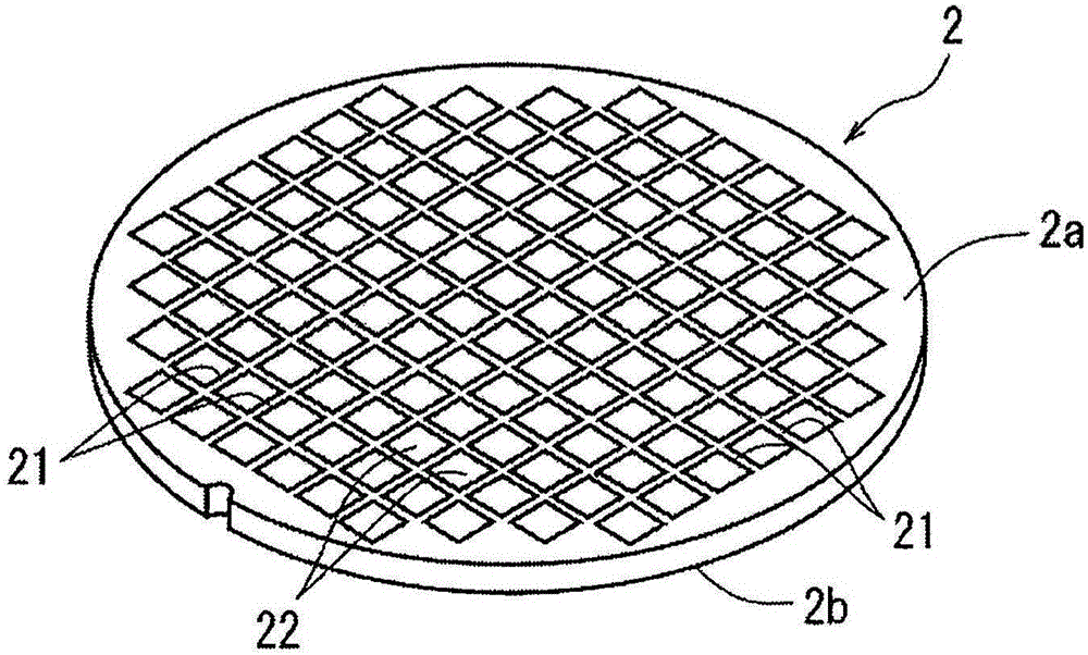
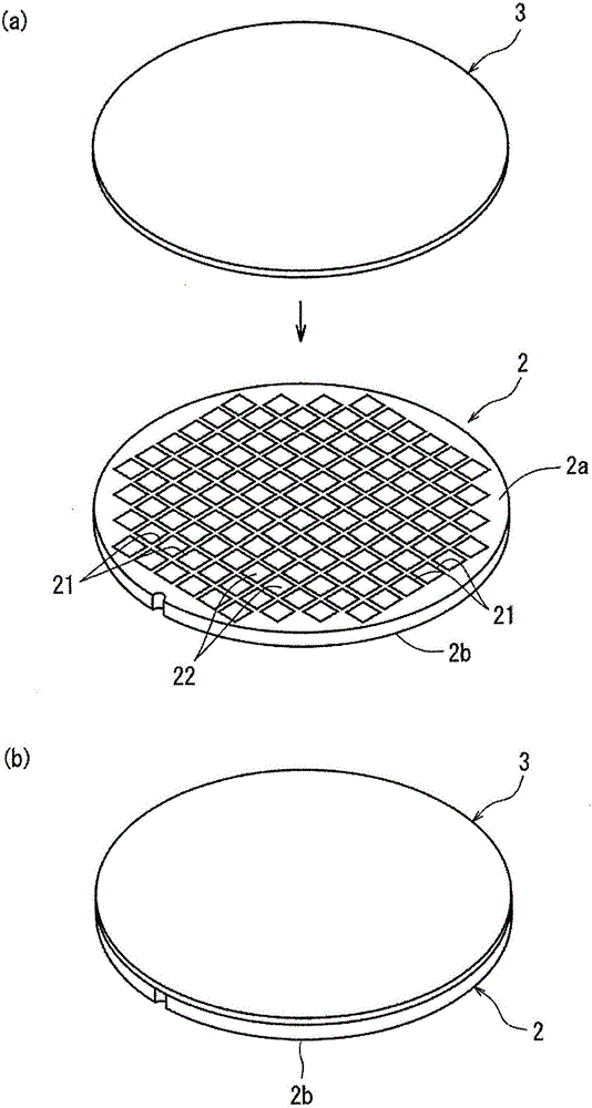
[0030] figure 1 A perspective view of a semiconductor wafer as a wafer processed according to the invention is shown. figure 1 The shown semiconductor wafer 2 is composed of a silicon wafer with a thickness of, for example, 500 μm, and a plurality of planned dividing lines 21 are formed in a grid pattern on the front surface 2 a, and formed in a plurality of regions divided by the plurality of planned dividing lines 21 . There are devices 22 such as ICs and LSIs. Hereinafter, a wafer processing method for dividing the semiconductor wafer 2 into individual devices 22 along the planned dividing lines 21 will be described.

[0031] First, in order to protect the devices 22 formed on the front surface 2 a of the semiconductor wafer 2 , an adhesive tape bonding step is performed to bond the adhesive tape to the front surfa...


PUM


Abstract

The invention provides a wafer processing method. A plurality of modified layers, which are not disposed in a wafer in a laminated manner, are capable of segmenting the wafer reliably. The wafer processing method comprises steps that the front surface of the wafer is provided with a plurality of segmentation predetermined lines in the shape of a grid, and the devices are formed on a plurality of areas divided by the above mentioned lines, and the wafer is segmented into various devices along the segmentation predetermined lines; according to an adhesive tape bonding process: the front surface of the wafer is provided with an adhesive tape in an adhesive manner; according to a modified layer forming process: the back surface side of the wafer is used to locate the focusing point of the pulse laser having the transmitting wavelength in the inner side, and is used to irradiate the pulse laser along the segmentation predetermined lines to form the modified layers; an adhesive tape heating process: the adhesive tape attached to the front surface of the wafer after the modified layer is heated, and then the cracks are extended from the modified layer to the front surface of the wafer; according to a segementation process: external force is applied to the wafer after the adhesive tape heating process, and then the wafer is segmented into various devices along the segmentation predetermined lines having the modified layers and the cracks.

Description

technical field [0001] The present invention relates to a wafer processing method, wherein a wafer having a plurality of planned dividing lines formed in a grid pattern on the front surface and devices formed in a plurality of regions divided by the plurality of planned dividing lines is divided along the planned dividing lines . Background technique [0002] In the manufacturing process of semiconductor devices, a plurality of regions are divided by dividing lines arranged in a grid on the front surface of a substantially disk-shaped semiconductor wafer, and devices such as ICs and LSIs are formed in the divided regions. The semiconductor wafer formed in this way is cut along the planned dividing lines to divide the regions where the devices are formed to manufacture individual devices. [0003] As a method of dividing wafers such as semiconductor wafers, a laser processing method called internal processing is put into practical use, using pulsed laser light with a wavelen...

Claims


Application Information

Patent Timeline
Patent Type & Authority Applications(China)
IPC IPC(8): H01L21/82
CPCH01L21/82H01L21/78H01L21/76H01L21/6836H01L21/268H01L21/324H01L21/304H01L21/30625
Inventor 中村胜
Owner DISCO CORP
Why Eureka
Try Eureka