Laminated wafer processing method and adhesive sheet

A processing method and adhesive sheet technology, which can be used in metal processing equipment, manufacturing tools, laser welding equipment, etc., and can solve the problems of inability to form a modified layer at the condensing point, inability to divide laminated chips, and insufficient depth.

Active Publication Date: 2018-09-11
DISCO CORP
View PDF9 Cites 1 Cited by
  • Summary
  • Abstract
  • Description
  • Claims
  • Application Information

AI Technical Summary

Problems solved by technology

However, in the stacked wafer, since the chip is not stacked on the outer peripheral portion, there is a step difference between the chip region and the outer peripheral portion on the interposer wafer side, so when the adhesive sheet is pasted on the chip side, the A phenomenon in which the outer peripheral portion of the interposer wafer is deflected toward the adhesive sheet side
[0010] In this way, when warping occurs in the outer peripheral portion of the interposer wafer, there arises a problem that, when the above-mentioned dividing starting point is formed and divided on the interposer wafer, the gap between the chip region and the outer peripheral portion cannot be properly aligned due to the amount of warping. The boundary portion forms the starting point of the split
For example, when the starting point of division is a modified layer obtained by irradiation with a laser beam, the focused point deviates and the modified layer cannot be formed. In addition, when the starting point of division is a groove obtained by laser processing or cutting, the depth of the groove will not be enough
In addition, even if a starting point for division is formed, in the wafer division method based on the expansion of the adhesive sheet described in Patent Document 4, the adhesive sheet cannot be sufficiently pasted on the outer peripheral portion of the interposer wafer due to the above-mentioned step difference. , at the boundary between the chip area and the outer periphery, the external force generated by the expansion is difficult to be transmitted to the boundary, and the stacked chips at the outermost periphery cannot be divided.

Method used


Image

  • Laminated wafer processing method and adhesive sheet
  • Laminated wafer processing method and adhesive sheet
  • Laminated wafer processing method and adhesive sheet

Examples


Embodiment Construction

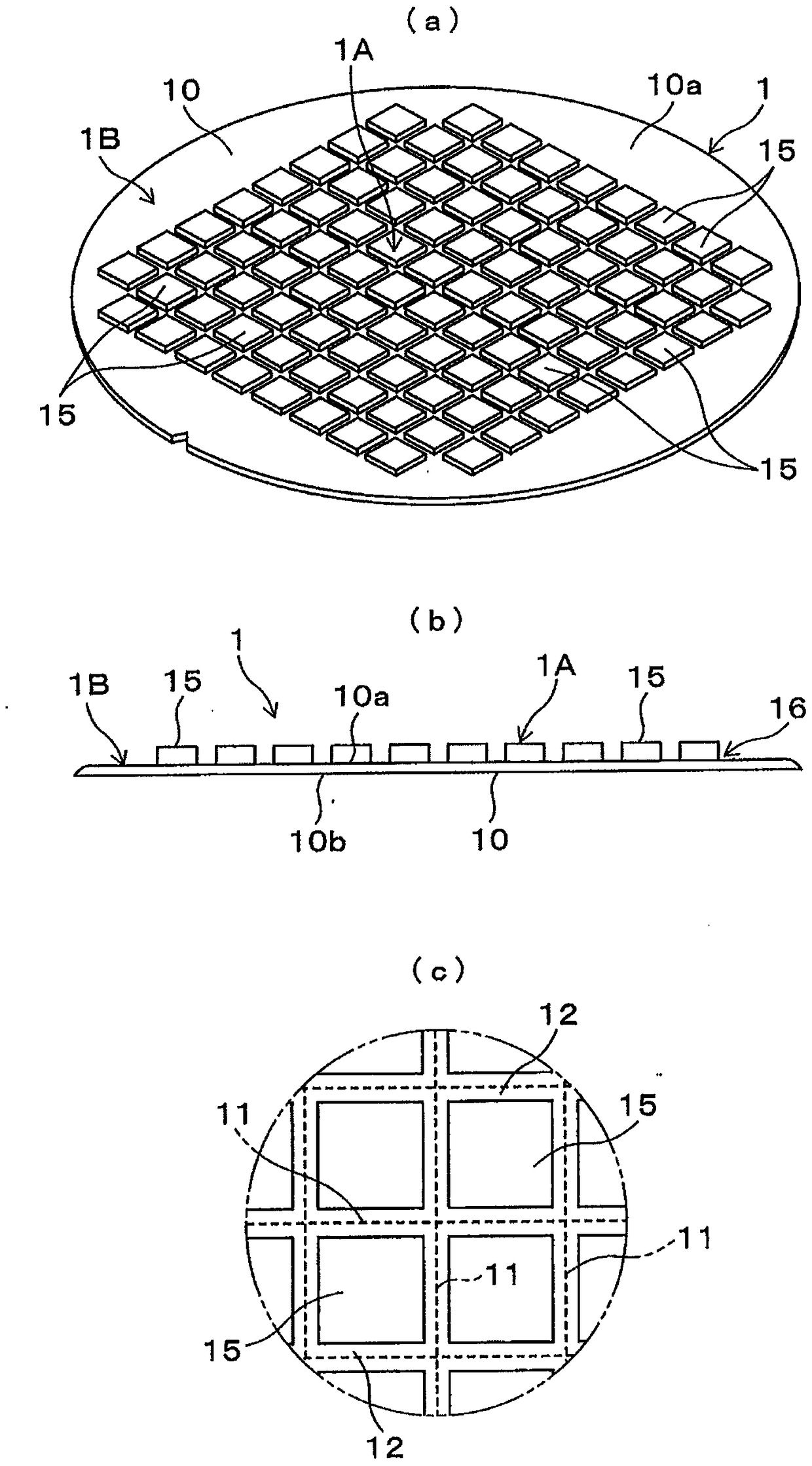
[0042] [1] Laminated wafer

[0043] figure 1 In one embodiment, a laminated wafer 1 divided into individual laminated chips is shown. The laminated wafer 1 has a plurality of rectangular chips 15 stacked on the surface 10a of a disk-shaped interposer wafer (hereinafter simply referred to as a wafer) 10 in which wiring, electrodes, etc. are incorporated. Chip 15 is a semiconductor device, etc., such as figure 1 As shown in (c), each chip 15 is stacked on each rectangular region 12 divided on the surface 10 a of the wafer 10 by grid-like dividing lines 11 . The wafer 10 is ground in advance on the back surface 10b side, and thinned to a predetermined thickness.

[0044]The laminated wafer 1 is divided into a substantially rectangular chip region 1A in which a plurality of chips 15 are laminated, and an outer peripheral remaining region 1B in which the outer peripheral portions of the chips 15 are not laminated. The thickness of the chip 15 is, for example, about 100 μm, ther...


PUM


Abstract

The invention provides a laminated wafer processing method and an adhesive piece. In a plurality of chip laminated wafers stacked on wafers, in a state of adhering chip sides on the adhesive piece, wafers can also be reliably cut into a plurality of laminated chips. A paste layer (22) of an adhesive piece (2) correspondingly forms projections (3) on the peripheral residual area (1B) of a paste layer (22) and a laminated wafer (1) is adhered to a chip (15) of the laminated wafer (1); the projections (3) and the peripheral residual area (1B) are correspondingly adhered on the surface (10a) of a wafer (10); the peripheral residual area (1B) of the wafer (10) is supported through the projections (3). In the state, a cutting start point (modified layer 10c) of the wafer (10) is formed along a cutting predetermined line (11), and the wafer (10) is applied with outer force through the expansion of the adhesive piece (2), and accordingly, a laminated chip (1c) on the outmost side can be cut the same as other laminated chips (1c).

Description

technical field [0001] The present invention relates to a method of processing a laminated wafer in which a plurality of chips are arranged on the wafer, and an adhesive sheet suitable for use in the processing method. Background technique [0002] As one of the methods for integrating multiple semiconductor devices into one package, three-dimensional mounting such as CoW (Chip on Wafer: chip on wafer) in which multiple semiconductor device chips are stacked and mounted in three-dimensional directions is known of. CoW forms a stacked chip in which chips are stacked on a chip by dividing a stacked wafer in which chips are stacked on a wafer for individual chips (see Patent Document 1). [0003] On the other hand, in order to divide such a wafer, dicing by machining is generally performed in which a cutting blade of a cutting device penetrates into the wafer (see Patent Document 2). In addition, in recent years, after a modified layer is formed inside a wafer by irradiation ...

Claims


Application Information

Patent Timeline
Patent Type & Authority Patents(China)
IPC IPC(8): H01L21/683H01L21/78B23K26/38
CPCB23K26/53H01L21/6836H01L21/78
Inventor 古田健次
Owner DISCO CORP
Why Eureka
Try Eureka